ZHCSOF3G April 2006 – July 2021 TLV320AIC3106
PRODUCTION DATA
- 1 特性
- 2 应用
- 3 说明
- 4 Revision History
- 5 说明(续)
- 6 Device Comparison Table
- 7 Pin Configuration and Functions
- 8 Specifications
- 9 Parameter Measurement Information
-
10Detailed Description
- 10.1 Overview
- 10.2 Functional Block Diagram
- 10.3
Feature Description
- 10.3.1 Hardware Reset
- 10.3.2 Digital Audio Data Serial Interface
- 10.3.3 Audio Data Converters
- 10.3.4 Audio Analog Inputs
- 10.3.5 Analog Fully Differential Line Output Drivers
- 10.3.6 Analog High Power Output Drivers
- 10.3.7 Input Impedance and VCM Control
- 10.3.8 General-Purpose I/O
- 10.3.9 Digital Microphone Connectivity
- 10.3.10 Micbias Generation
- 10.3.11 Short Circuit Output Protection
- 10.3.12 Jack/Headset Detection
- 10.4 Device Functional Modes
- 10.5 Programming
- 10.6 Register Maps
- 11Application and Implementation
- 12Power Supply Recommendations
- 13Layout
- 14Device and Documentation Support
封装选项
请参考 PDF 数据表获取器件具体的封装图。
机械数据 (封装 | 引脚)
- RGZ|48
- ZXH|80
散热焊盘机械数据 (封装 | 引脚)
- RGZ|48
订购信息
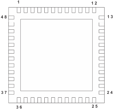
7 Pin Configuration and Functions

Solder the VQFN thermal
pad to the ground plane (DRVSS).
Figure 7-1 RGZ
Package,48-Pin VQFN,Bottom View
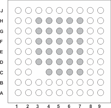
The shaded balls are not
connected to the die, but are electrically connected to each other. Is recommended to
solder them to analog ground in order to enhance the thermal performance of the
device.
Figure 7-2 ZQE
Package,80-Ball BGA Microstar Junior,Bottom ViewTable 7-1 Pin Functions
| PIN | I/O | DESCRIPTION | ||
|---|---|---|---|---|
| NAME | VQFN | BGA BALL | ||
| MICBIAS | 13 | A2 | O | Microphone bias voltage output |
| MIC3R | 14 | A1 | I | MIC3 input (right or multifunction) |
| AVSS_ADC | 15 | C2,D2 | – | Analog ADC ground supply, 0 V |
| DRVDD | 16,17 | B1,C1 | – | ADC analog and output driver voltage supply, 2.7 V–3.6 V |
| HPLOUT | 18 | D1 | O | High-power output driver (left +) |
| HPLCOM | 19 | E1 | O | High-power output driver (left – or multifunctional) |
| DRVSS | 20,21 | E2,F2 | – | Analog output driver ground supply, 0 V |
| HPRCOM | 22 | F1 | O | High-power output driver (right – or multifunctional) |
| HPROUT | 23 | G1 | O | High-power output driver (right +) |
| DRVDD | 24 | H1 | – | ADC analog and output driver voltage supply, 2.7 V–3.6 V |
| AVDD_DAC | 25 | J1 | – | Analog DAC voltage supply, 2.7 V–3.6 V |
| AVSS_DAC | 26 | G2,H2 | – | Analog DAC ground supply, 0 V |
| MONO_LOP | 27 | J2 | O | Mono line output (+) |
| MONO_LOM | 28 | J3 | O | Mono line output (–) |
| LEFT_LOP | 29 | J4 | O | Left line output (+) |
| LEFT_LOM | 30 | J5 | O | Left line output (–) |
| RIGHT_LOP | 31 | J6 | O | Right line output (+) |
| RIGHT_LOM | 32 | J7 | O | Right line output (–) |
| RESET | 33 | H8 | I | Reset |
| GPIO2 | 34 | J8 | I/O | General-purpose input/output #2 (input/output)/digital microphone data input/PLL clock input/audio serial data bus bit clock input/output |
| GPIO1 | 35 | J9 | I/O | General-purpose input/output #1 (input/output)/PLL/clock mux output/short circuit interrupt/AGC noise flag/digital microphone clock audio serial data bus word clock input/output |
| DVDD | 36 | H9 | – | Digital core voltage supply, 1.65 V–1.95 V |
| MCLK | 37 | G8 | I | Master clock input |
| BCLK | 38 | G9 | I | Audio serial data bus bit clock (input/output) |
| WCLK | 39 | F9 | I | Audio serial data bus word clock (input/output) |
| DIN | 40 | E9 | I | Audio serial data bus data input (input) |
| DOUT | 41 | F8 | O | Audio serial data bus data output (output) |
| DVSS | 42 | D9 | – | Digital core / I/O ground supply, 0V |
| SELECT | 43 | E8 | I | Control mode select pin (1 = SPI, 0 = I2C) |
| IOVDD | 44 | C9 | – | I/O voltage supply, 1.1 V–3.6 V |
| MFP0 | 45 | B8 | I | Multifunction pin #0 – SPI chip select / GPI / I2C address pin #0 |
| MFP1 | 46 | B9 | I | Multifunction pin #1 – SPI serial clock / GPI / I2C address pin #1S |
| MFP2 | 47 | A8 | I | Multifunction pin #2 – SPI MISO slave serial data output / GPOI |
| MFP3 | 48 | A9 | I | Multifunction pin #3 – SPI MOSI slave serial data input/GPI/audio serial data bus data input |
| SCL | 1 | C8 | I/O | I2C serial clock/GPIO |
| SDA | 2 | D8 | I/O | I2C serial data input/output/GPIO |
| NC | – | A7 | – | Not connected |
| LINE1LP | 3 | A6 | I | MIC1 or Line1 analog input (left + or multifunction) |
| LINE1LM | 4 | A5 | I | MIC1 or Line1 analog input (left – or multifunction) |
| LINE1RP | 5 | B7 | I | MIC1 or Line1 analog input (right + or multifunction) |
| LINE1RM | 6 | B6 | I | MIC1 or Line1 analog input (right – or multifunction) |
| LINE2LP | 7 | A4 | I | MIC2 or Line2 analog input (left + or multifunction) |
| LINE2LM | 8 | B5 | I | MIC2 or Line2 analog input (left – or multifunction) |
| LINE2RP | 9 | B4 | I | MIC2 or Line2 analog input (right + or multifunction) |
| LINE2RM | 10 | A3 | I | MIC2 or Line2 analog input (right – or multifunction) |
| MIC3L | 11 | B3 | I | MIC3 input (left or multifunction) |
| MICDET | 12 | B2 | I | Microphone detect |
| NC | – | C4-C7, D3-D7, E3-E7, F3-F7, G3-G7, H3-H7 |
– | Not connected |