ZHCSOF3G April 2006 – July 2021 TLV320AIC3106
PRODUCTION DATA
- 1 特性
- 2 应用
- 3 说明
- 4 Revision History
- 5 说明(续)
- 6 Device Comparison Table
- 7 Pin Configuration and Functions
- 8 Specifications
- 9 Parameter Measurement Information
-
10Detailed Description
- 10.1 Overview
- 10.2 Functional Block Diagram
- 10.3
Feature Description
- 10.3.1 Hardware Reset
- 10.3.2 Digital Audio Data Serial Interface
- 10.3.3 Audio Data Converters
- 10.3.4 Audio Analog Inputs
- 10.3.5 Analog Fully Differential Line Output Drivers
- 10.3.6 Analog High Power Output Drivers
- 10.3.7 Input Impedance and VCM Control
- 10.3.8 General-Purpose I/O
- 10.3.9 Digital Microphone Connectivity
- 10.3.10 Micbias Generation
- 10.3.11 Short Circuit Output Protection
- 10.3.12 Jack/Headset Detection
- 10.4 Device Functional Modes
- 10.5 Programming
- 10.6 Register Maps
- 11Application and Implementation
- 12Power Supply Recommendations
- 13Layout
- 14Device and Documentation Support
封装选项
请参考 PDF 数据表获取器件具体的封装图。
机械数据 (封装 | 引脚)
- RGZ|48
- ZXH|80
散热焊盘机械数据 (封装 | 引脚)
- RGZ|48
订购信息
10.3.2.5 TDM Data Transfer
Time-division multiplexed data transfer can be realized in any of the above transfer modes if the 256-clock bit clock mode is selected, although it is recommended to be used in either left-justified mode or DSP mode. By changing the programmable offset, the bit clock in each frame where the data begins can be changed, and the serial data output driver (DOUT) can also be programmed to 3-state during all bit clocks except when valid data is being put onto the bus. This allows other codecs to be programmed with different offsets and to drive their data onto the same DOUT line, just in a different slot. For incoming data, the codec simply ignores data on the bus except where it is expected based on the programmed offset.
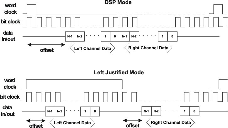
Note that the location of the data when an offset is programmed is different, depending on what transfer mode is selected. In DSP mode, both left and right channels of data are transferred immediately adjacent to each other in the frame. This differs from left-justified mode, where the left and right channel data will always be a half-frame apart in each frame. In this case, as the offset is programmed from zero to some higher value, both the left and right channel data move across the frame, but still stay a full half-frame apart from each other. This is depicted in Figure 10-7 for the two cases.
 Figure 10-7 DSP Mode and Left Justified Modes, Showing the Effect of a Programmed Data Word Offset