ZHCSOF3G April 2006 – July 2021 TLV320AIC3106
PRODUCTION DATA
- 1 特性
- 2 应用
- 3 说明
- 4 Revision History
- 5 说明(续)
- 6 Device Comparison Table
- 7 Pin Configuration and Functions
- 8 Specifications
- 9 Parameter Measurement Information
-
10Detailed Description
- 10.1 Overview
- 10.2 Functional Block Diagram
- 10.3
Feature Description
- 10.3.1 Hardware Reset
- 10.3.2 Digital Audio Data Serial Interface
- 10.3.3 Audio Data Converters
- 10.3.4 Audio Analog Inputs
- 10.3.5 Analog Fully Differential Line Output Drivers
- 10.3.6 Analog High Power Output Drivers
- 10.3.7 Input Impedance and VCM Control
- 10.3.8 General-Purpose I/O
- 10.3.9 Digital Microphone Connectivity
- 10.3.10 Micbias Generation
- 10.3.11 Short Circuit Output Protection
- 10.3.12 Jack/Headset Detection
- 10.4 Device Functional Modes
- 10.5 Programming
- 10.6 Register Maps
- 11Application and Implementation
- 12Power Supply Recommendations
- 13Layout
- 14Device and Documentation Support
封装选项
请参考 PDF 数据表获取器件具体的封装图。
机械数据 (封装 | 引脚)
- RGZ|48
- ZXH|80
散热焊盘机械数据 (封装 | 引脚)
- RGZ|48
订购信息
10.3.6 Analog High Power Output Drivers
The TLV320AIC3106 includes four high power output drivers with extensive flexibility in their usage. These output drivers are individually capable of driving 30 mW each into a 16-Ω load in single-ended configuration, and they can be used in pairs connected in bridge-terminated load (BTL) configuration between two driver outputs.
The high power output drivers can be configured in a variety of ways, including:
- driving up to two fully differential output signals
- driving up to four single-ended output signals
- driving two single-ended output signals, with one or two of the remaining drivers driving a fixed VCM level, for a pseudo-differential stereo output
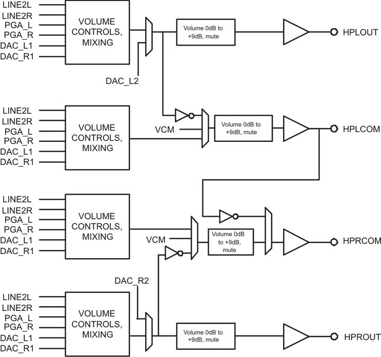
The output stage architecture leading to the high power output drivers is shown in Figure 10-16, with the volume control and mixing blocks being effectively identical to that shown in Figure 10-15. Note that each of these drivers have a output level control block like those included with the line output drivers, allowing gain adjustment up to +9dB on the output signal. As in the previous case, this output level adjustment is not intended to be used as a standard volume control, but instead is included for additional fullscale output signal level control.
Two of the output drivers, HPROUT and HPLOUT, include a direct connection path for the stereo DAC outputs to be passed directly to the output drivers and bypass the analog volume controls and mixing networks, using the DAC_L2/R2 path. As in the line output case, this functionality provides the highest quality DAC playback performance with reduced power dissipation, but can only be utilized if the DAC output does not need to route to multiple output drivers simultaneously, and if mixing of the DAC output with other analog signals is not needed.
 Figure 10-16 Architecture of the Output Stage Leading to the High Power Output Drivers
The high power output drivers include additional circuitry to avoid artifacts on the audio output during power-on and power-off transient conditions. The user should first program the type of output configuration being used in Page-0/Reg-14, to allow the device to select the optimal power-up scheme to avoid output artifacts. The power-up delay time for the high power output drivers is also programmable over a wide range of time delays, from instantaneous up to 4-sec, using Page-0/Reg-42.
When these output drivers are powered down, they can be placed into a variety of output conditions based on register programming. If lowest power operation is desired, then the outputs can be placed into a 3-state condition, and all power to the output stage is removed. However, this generally results in the output nodes drifting to rest near the upper or lower analog supply, due to small leakage currents at the pins. This then results in a longer delay requirement to avoid output artifacts during driver power-on. In order to reduce this required power-on delay, the TLV320AIC3106 includes an option for the output pins of the drivers to be weakly driven to the VCM level they would normally rest at when powered with no signal applied. This output VCM level is determined by an internal bandgap voltage reference, and thus results in extra power dissipation when the drivers are in powerdown. However, this option provides the fastest method for transitioning the drivers from powerdown to full power operation without any output artifact introduced.
The device includes a further option that falls between the other two – while it requires less power drawn while the output drivers are in powerdown, it also takes a slightly longer delay to power-up without artifact than if the bandgap reference is kept alive. In this alternate mode, the powered-down output driver pin is weakly driven to a voltage of approximately half the DRVDD1/2 supply level using an internal voltage divider. This voltage will not match the actual VCM of a fully powered driver, but due to the output voltage being close to its final value, a much shorter power-up delay time setting can be used and still avoid any audible output artifacts. These output voltage options are controlled in Page-0/Reg-42.
The high power output drivers can also be programmed to power up first with the output level control in a highly attenuated state, then the output driver will automatically slowly reduce the output attenuation to reach the desired output level setting programmed. This capability is enabled by default but can be enabled in Page-0/Reg-40.