ZHCSOF3G April 2006 – July 2021 TLV320AIC3106
PRODUCTION DATA
- 1 特性
- 2 应用
- 3 说明
- 4 Revision History
- 5 说明(续)
- 6 Device Comparison Table
- 7 Pin Configuration and Functions
- 8 Specifications
- 9 Parameter Measurement Information
-
10Detailed Description
- 10.1 Overview
- 10.2 Functional Block Diagram
- 10.3
Feature Description
- 10.3.1 Hardware Reset
- 10.3.2 Digital Audio Data Serial Interface
- 10.3.3 Audio Data Converters
- 10.3.4 Audio Analog Inputs
- 10.3.5 Analog Fully Differential Line Output Drivers
- 10.3.6 Analog High Power Output Drivers
- 10.3.7 Input Impedance and VCM Control
- 10.3.8 General-Purpose I/O
- 10.3.9 Digital Microphone Connectivity
- 10.3.10 Micbias Generation
- 10.3.11 Short Circuit Output Protection
- 10.3.12 Jack/Headset Detection
- 10.4 Device Functional Modes
- 10.5 Programming
- 10.6 Register Maps
- 11Application and Implementation
- 12Power Supply Recommendations
- 13Layout
- 14Device and Documentation Support
封装选项
请参考 PDF 数据表获取器件具体的封装图。
机械数据 (封装 | 引脚)
- RGZ|48
- ZXH|80
散热焊盘机械数据 (封装 | 引脚)
- RGZ|48
订购信息
10.3.2 Digital Audio Data Serial Interface
Audio data is transferred between the host processor and the TLV320AIC3106 via the digital audio data serial interface, or audio bus. The audio bus on this device is very flexible, including left or right justified data options, support for I2S or PCM protocols, programmable data length options, a TDM mode for multichannel operation, very flexible master/slave configurability for each bus clock line, and the ability to communicate with multiple devices within a system directly.
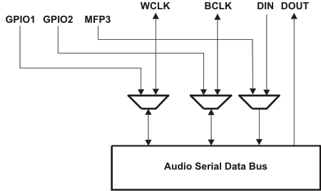
The data serial interface uses two sets of pins for communication between external devices, with the particular pin used controlled through register programming. This configuration is illustrated in Figure 10-1.
 Figure 10-1 Alternate Audio Bus Mulitplexing Function
In cases where MFP3 is needed for a secondary device digital input, the TLV320AIC3106 must be used in I2C mode (when in SPI mode, MFP3 is used as the SPI bus MOSI pin and thus cannot be used here as an alternate digital input source).
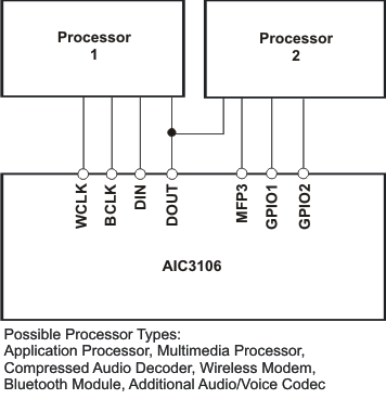
This mux capability allows the TLV320AIC3106 to communicate with two separate devices with independent I2S/PCM buses. An example of such an application is a cellphone containing a Bluetooth transceiver with PCM/I2S interface, as shown in Figure 10-2. The applications processor can be connected to the WCLK, BCLK, DIN, DOUT pins on the TLV320AIC3106, while a Bluetooth device with PCM interface can be connected to the GPIO1, GPIO2, MFP3, and DOUT pins on the TLV320AIC3106. By programming the registers via I2C control, the applications processor can determine which device is communicating with the TLV320AIC3106. This is attractive in cases where the TLV320AIC3106 can be configured to communicate data with the Bluetooth device, then the applications processor can be put into a low power sleep mode, while voice/audio transmission still occurs between the Bluetooth device and the TLV320AIC3106.
 Figure 10-2 TLV320AIC3106 Connected to Multiple Audio Devices
The audio bus of the TLV320AIC3106 can be configured for left or right justified, I2S, DSP, or TDM modes of operation, where communication with standard telephony PCM interfaces is supported within the TDM mode. These modes are all MSB-first, with data width programmable as 16, 20, 24, or 32 bits. In addition, the word clock (WCLK or GPIO1) and bit clock (BCLK or GPIO2) can be independently configured in either Master or Slave mode, for flexible connectivity to a wide variety of processors
The word clock (WCLK or GPIO1) is used to define the beginning of a frame, and may be programmed as either a pulse or a square-wave signal. The frequency of this clock corresponds to the maximum of the selected ADC and DAC sampling frequencies.
The bit clock (BCLK or GPIO2) is used to clock in and out the digital audio data across the serial bus. When in Master mode, this signal can be programmed in two further modes: continuous transfer mode, and 256-clock mode. In continuous transfer mode, only the minimal number of bit clocks needed to transfer the audio data are generated, so in general the number of bit clocks per frame will be two times the data width. For example, if data width is chosen as 16 bits, then 32 bit clocks will be generated per frame. If the bit clock signal in master mode will be used by a PLL in another device, it is recommended that the 16-bit or 32-bit data width selections be used. These cases result in a low jitter bit clock signal being generated, having frequencies of 32 × fS or 64 × fS. In the cases of 20-bit and 24-bt data width in master mode, the bit clocks generated in each frame will not all be of equal period, due to the device not having a clean 40 × fS or 48 × fS clock signal readily available. The average frequency of the bit clock signal is still accurate in these cases (being 40 × fS or 48 × fS), but the resulting clock signal has higher jitter than in the 16-bit and 32-bit cases.
In 256-clock mode, a constant 256 bit clocks per frame are generated, independent of the data width chosen. The TLV320AIC3106 further includes programmability to 3-state the DOUT line during all bit clocks when valid data is not being sent. By combining this capability with the ability to program at what bit clock in a frame the audio data will begin, time-division multiplexing (TDM) can be accomplished, resulting in multiple codecs able to use a single audio serial data bus.
When the audio serial data bus is powered down while configured in master mode, the pins associated with the interface will be put into a 3-state output condition.