ZHCSE78A December 2011 – September 2015 TLV320AIC3262
PRODUCTION DATA.
- 1 特性
- 2 应用范围
- 3 说明
- 4 修订历史记录
- 5 说明 (续)
- 6 Device Comparison Table
- 7 Pin Configuration and Functions
-
8 Specifications
- 8.1 Absolute Maximum Ratings
- 8.2 ESD Ratings
- 8.3 Recommended Operating Conditions
- 8.4 Thermal Information
- 8.5 Electrical Characteristics, SAR ADC
- 8.6 Electrical Characteristics, ADC
- 8.7 Electrical Characteristics, Bypass Outputs
- 8.8 Electrical Characteristics, Microphone Interface
- 8.9 Electrical Characteristics, Audio DAC Outputs
- 8.10 Electrical Characteristics, Class-D Outputs
- 8.11 Electrical Characteristics, Miscellaneous
- 8.12 Electrical Characteristics, Logic Levels
- 8.13 I2S/LJF/RJF Timing in Master Mode (see )
- 8.14 I2S/LJF/RJF Timing in Slave Mode (see )
- 8.15 DSP/Mono PCM Timing in Slave Mode (see )
- 8.16 I2C Interface Timing (see )
- 8.17 SPI Interface Timing
- 8.18 Dissipation Ratings
- 8.19 Typical Characteristics
- 9 Parameter Measurement Information
-
10Detailed Description
- 10.1 Overview
- 10.2 Functional Block Diagram
- 10.3
Feature Description
- 10.3.1 Digital Pins
- 10.3.2 Analog Pins
- 10.3.3 Multifunction Pins
- 10.3.4
Analog Audio I/O
- 10.3.4.1 Analog Low Power Bypass
- 10.3.4.2 ADC Bypass Using Mixer Amplifiers
- 10.3.4.3 Headphone Outputs
- 10.3.4.4 Using the Headphone Amplifier
- 10.3.4.5 Ground-Centered Headphone Amplifier Configuration
- 10.3.4.6 Circuit Topology
- 10.3.4.7 Charge Pump Set-Up and Operation
- 10.3.4.8 Output Power Optimization
- 10.3.4.9 Offset Correction and Start-Up
- 10.3.4.10 Ground-Centered Headphone Setup
- 10.3.4.11 Stereo Unipolar Configuration
- 10.3.4.12 Mono Differential DAC to Mono Differential Headphone Output
- 10.3.4.13 Stereo Line Outputs
- 10.3.4.14 Line Out Amplifier Configurations
- 10.3.4.15 Differential Receiver Output
- 10.3.4.16 Stereo Class-D Speaker Outputs
- 10.3.5 ADC / Digital Microphone Interface
- 10.3.6 DAC
- 10.3.7 Powertune
- 10.3.8 Clock Generation and PLL
- 10.3.9 Interfaces
- 10.3.10 Device Special Functions
- 10.3.11 Device Power Consumption
- 10.3.12 Powertune
- 10.3.13 Clock Generation and PLL
- 10.3.14 Interfaces
- 10.3.15 miniDSP
- 10.3.16 Device Special Functions
- 10.4 Device Functional Modes
- 10.5 Register Maps
- 11Application and Implementation
- 12Power Supply Recommendations
- 13Layout
- 14器件和文档支持
- 15机械、封装和可订购信息
8 Specifications
8.1 Absolute Maximum Ratings
over operating free-air temperature range (unless otherwise noted) (1)| MIN | MAX | UNIT | ||
|---|---|---|---|---|
| AVDD1_18, AVDD2_18, AVDD4_18, AVDD_18 to AVSS1, AVSS2, AVSS4, AVSS respectively(2) | –0.3 | 2.2 | V | |
| AVDD3_33 to AVSS3 and RECVDD_33 to RECVSS | –0.3 | 3.9 | V | |
| DVDD to DVSS | –0.3 | 2.2 | V | |
| IOVDD to IOVSS | –0.3 | 3.9 | V | |
| HVDD_18 to AVSS | –0.3 | 2.2 | V | |
| CPVDD_18 to CPVSS | –0.3 | 2.2 | V | |
| SLVDD to SLVSS, SRVDD to SRVSS, SPK_V to SRVSS(3) | –0.3 | 6 | V | |
| Digital Input voltage to ground | IOVSS – 0.3 | IOVDD + 0.3 | V | |
| Analog input voltage to ground | AVSS – 0.3 | AVDDx_18 + 0.3 | V | |
| VBAT | –0.3 | 6 | V | |
| Operating temperature | –40 | 85 | °C | |
| Junction temperature (TJ Max) | 105 | °C | ||
| Storage temperature, Tstg | –55 | 125 | °C | |
(1) Stresses beyond those listed under Absolute Maximum Ratings may cause permanent damage to the device. These are stress ratings only, which do not imply functional operation of the device at these or any other conditions beyond those indicated under Recommended Operating Conditions. Exposure to absolute-maximum-rated conditions for extended periods may affect device reliability.
(2) TI recommends to keep all AVDDx_18 supplies within ± 50 mV of each other.
(3) TI recommends to keep SLVDD, SRVDD, and SPK_V supplies within ± 50 mV of each other.
8.2 ESD Ratings
| VALUE | UNIT | |||
|---|---|---|---|---|
| V(ESD) | Electrostatic discharge | Human body model (HBM), per ANSI/ESDA/JEDEC JS-001(1) | ±2400 | V |
| Charged-device model (CDM), per JEDEC specification JESD22-C101(2) | ±1000 | |||
(1) JEDEC document JEP155 states that 500-V HBM allows safe manufacturing with a standard ESD control process.
(2) JEDEC document JEP157 states that 250-V CDM allows safe manufacturing with a standard ESD control process.
8.3 Recommended Operating Conditions
| MIN | NOM | MAX | UNIT | ||||
|---|---|---|---|---|---|---|---|
| AVDD1_18, AVDD2_18, AVDD4_18, AVDD_18 | Power Supply Voltage Range | Referenced to AVSS1, AVSS2, AVSS4, AVSS respectively(1) It is recommended to connect each of these supplies to a single supply rail. | 1.5 | 1.8 | 1.95 | V | |
| AVDD3_33 , RECVDD_33 | Referenced to AVSS3 and RECVSS respectively | 1.65(3) | 3.3 | 3.6 | |||
| IOVDD | Referenced to IOVSS(1) | 1.1 | 3.6 | ||||
| DVDD(2) | Referenced to DVSS(1) | 1.26 | 1.8 | 1.95 | |||
| CPVDD_18 | Power Supply Voltage Range | Referenced to CPVSS (1) | 1.26 | 1.8 | 1.95 | V | |
| HVDD_18 | Referenced to AVSS(1) | Ground-centered Configuration | 1.5(3) | 1.8 | 1.95 | ||
| Unipolar Configuration | 1.65(3) | 3.6 | |||||
| SLVDD(1) | Power Supply Voltage Range | Referenced to SLVSS(1) | 2.7 | 5.5 | V | ||
| SRVDD(1) | Power Supply Voltage Range | Referenced to SRVSS(1) | 2.7 | 5.5 | V | ||
| SPK_V(1) | Power Supply Voltage Range | Referenced to SRVSS(1) | 2.7 | 5.5 | V | ||
| VREF_SAR | External voltage reference for SAR | Referenced to AVSS | 1.8 | AVDDx_18 | V | ||
| PLL Input Frequency(4) | Clock divider uses fractional divide (D > 0), P=1, PLL_CLKIN_DIV=1, DVDD ≥ 1.65 V (Refer to table in SLAU309, Maximum TLV320AIC3262 Clock Frequencies) |
10 | 20 | MHz | |||
| Clock divider uses integer divide (D = 0), P=1, PLL_CLKIN_DIV=1, DVDD ≥ 1.65 V (Refer to table in SLAU309, Maximum TLV320AIC3262 Clock Frequencies) |
0.512 | 20 | MHz | ||||
| MCLK | Master Clock Frequency | MCLK; Master Clock Frequency; IOVDD ≥ 1.65 V | 50 | MHz | |||
| MCLK; Master Clock Frequency; IOVDD ≥ 1.1 V | 33 | ||||||
| SCL | SCL Clock Frequency | 400 | kHz | ||||
| LOL, LOR | Stereo line output load resistance | 0.6 | 10 | kΩ | |||
| HPL, HPR | Stereo Headphone Output Load Resistance | Single-ended configuration | 14.4 | 16 | Ω | ||
| SPKLP-SPKLM, SPKRP-SPKRM | Speaker Output Load Resistance | Differential | 7.2 | 8 | Ω | ||
| RECP-RECM | Receiver output resistance | Differential | 24.4 | 32 | Ω | ||
| CIN | Charge Pump Input Capacitor (CPVDD to CPVSS Pins) | 10 | µF | ||||
| CO | Charge Pump Output Capacitor (VNEG Pin) | Type X7R | 2.2 | µF | |||
| CF | Charge Pump Flying Capacitor (CPFCP to CPFCM Pins) | Type X7R | 2.2 | µF | |||
| TOPR | Operating Temperature Range | –40 | 85 | °C | |||
(1) All grounds on board are tied together, so they should not differ in voltage by more than 0.1 V max, for any combination of ground signals. AVDDx_18 are within ±0.05 V of each other. SLVDD, SRVDD, and SPK_V are within ±0.05 V of each other.
(2) At DVDD values lower than 1.65V, the PLL does not function. Please see table in SLAU309, Maximum TLV320AIC3262 Clock Frequencies for details on maximum clock frequencies.
(3) Minimum voltage for HVDD_18 and RECVDD_33 should be greater than or equal to AVDD2_18. Minimum voltage for AVDD3_33 should be greater than or equal to AVDD1_18 and AVDD2_18.
(4) The PLL Input Frequency refers to clock frequency after PLL_CLKIN_DIV divider. Frequencies higher than 20 MHz can be sent as an input to this PLL_CLKIN_DIV and reduced in frequency prior to input to the PLL.
8.4 Thermal Information
| THERMAL METRIC(1) | TLV320AIC3262 | UNIT | |
|---|---|---|---|
| YZF (DSBGA) | |||
| 81 PINS | |||
| RθJA | Junction-to-ambient thermal resistance | 39.1 | °C/W |
| RθJC(top) | Junction-to-case (top) thermal resistance | 0.1 | °C/W |
| RθJB | Junction-to-board thermal resistance | 12.0 | °C/W |
| ψJT | Junction-to-top characterization parameter | 0.7 | °C/W |
| ψJB | Junction-to-board characterization parameter | 11.5 | °C/W |
(1) For more information about traditional and new thermal metrics, see the Semiconductor and IC Package Thermal Metrics application report, SPRA953.
8.5 Electrical Characteristics, SAR ADC
TA = 25°C; AVDD_18, AVDDx_18, HVDD_18, CPVDD_18, DVDD, IOVDD = 1.8V; AVDD3_33, RECVDD_33 = 3.3V; SLVDD, SRVDD, SPK_V = 3.6V; fS (Audio) = 48kHz; Audio Word Length = 16 bits; Cext = 1μF on VREF_SAR and VREF_AUDIO pins; PLL disabled unless otherwise noted.| PARAMETER | TEST CONDITIONS | MIN | TYP | MAX | UNIT | |
|---|---|---|---|---|---|---|
| SAR ADC INPUTS | ||||||
| Analog Input | Input voltage range | IN1L/AUX1 or IN1R/AUX2 Selected | 0 | VREF_SAR | V | |
| Input impedance | 1 ÷ (f × CSAR_IN)(1) | kΩ | ||||
| Input capacitance, CSAR_IN | 25 | pF | ||||
| Input leakage current | 1 | µA | ||||
| Battery Input | VBAT Input voltage range | VBAT (Battery measurement) selected | 2.2 | 5.5 | V | |
| VBAT Input impedance | 5 | kΩ | ||||
| VBAT Input capacitance | 25 | pF | ||||
| VBAT Input leakage current | 1 | µA | ||||
| SAR ADC CONVERSION | ||||||
| Resolution | Programmable: 8-bit, 10-bit, 12-bit | 8 | 12 | Bits | ||
| No missing codes | 12-bit resolution | 11 | Bits | |||
| IN1L/ AUX1 |
Integral linearity | 12-bit resolution, SAR ADC clock = Internal Oscillator Clock, Conversion clock = Internal Oscillator / 4, External Reference = 1.8 V(3) | ±1 | LSB | ||
| Offset error | ±1 | LSB | ||||
| Gain error | 0.07% | |||||
| Noise | DC voltage applied to IN1L/AUX1 = 1 V, SAR ADC clock = Internal Oscillator Clock, Conversion clock = Internal Oscillator / 4, External Reference = 1.8 V(2)(3) | ±1 | LSB | |||
| VBAT | Accuracy | 12-bit resolution, SAR ADC clock = Internal Oscillator Clock, Conversion clock = Internal Oscillator / 4, Internal Reference = 1.25 V | 2% | |||
| Offset error | ±2 | LSB | ||||
| Gain error | 1.5% | |||||
| Noise | DC voltage applied to VBAT = 3.6 V, 12-bit resolution, SAR ADC clock = Internal Oscillator Clock, Conversion clock = Internal Oscillator / 4, Internal Reference = 1.25 V | ±0.5 | LSB | |||
| CONVERSION RATE | ||||||
| Normal conversion operation | 12-bit resolution, SAR ADC clock = 12 MHz External Clock, Conversion clock = External Clock / 4, External Reference = 1.8 V(3). With Fast SPI reading of data. | 119 | kHz | |||
| High-speed conversion operation | 8-bit resolution,SAR ADC clock = 12 MHz External Clock, Internal Conversion clock = External Clock (Conversion accuracy is reduced.), External Reference = 1.8 V(3). With Fast SPI reading of data. | 250 | kHz | |||
| VOLTAGE REFERENCE - VREF_SAR | ||||||
| Voltage range | Internal VREF_SAR | 1.25 ± 0.05 | V | |||
| External VREF_SAR | 1.25 | AVDDx_18 | V | |||
| Reference Noise | CM=0.9V, Cref = 1 μF | 32 | μVRMS | |||
| Decoupling Capacitor | 1 | μF | ||||
(1) SAR input impedance is dependent on the sampling frequency (f designated in Hz), and the sampling capacitor is CSAR_IN = 25 pF.
(2) Noise from external reference voltage is excluded from this measurement.
(3) When utilizing External SAR reference, this external reference should be restricted VEXT_SAR_REF ≤ AVDD_18 and AVDD2_18.
8.6 Electrical Characteristics, ADC
TA = 25°C; AVDD_18, AVDDx_18, HVDD_18, CPVDD_18, DVDD, IOVDD = 1.8V; AVDD3_33, RECVDD_33 = 3.3V; SLVDD, SRVDD, SPK_V = 3.6V; fS (Audio) = 48kHz; Audio Word Length = 16 bits; Cext = 1μF on VREF_SAR and VREF_AUDIO pins; PLL disabled unless otherwise noted.| PARAMETER | TEST CONDITIONS | MIN | TYP | MAX | UNIT | |
|---|---|---|---|---|---|---|
| AUDIO ADC (CM = 0.9 V) (1) (2) | ||||||
| Input signal level (0dB) | Single-ended, CM = 0.9 V | 0.5 | VRMS | |||
| Device Set-up | 1-kHz sine wave input, Single-ended Configuration IN2R to Right ADC and IN2L to Left ADC, Rin = 20 kΩ, fs = 48 kHz, AOSR = 128, MCLK = 256*fs, PLL Disabled; AGC = OFF, Channel Gain = 0 dB, Processing Block = PRB_R1, Power Tune = PTM_R4 |
|||||
| SNR | Signal-to-noise ratio, A-weighted(1) (2) | Inputs AC-shorted to ground | 85 | 93 | dB | |
| IN1R, IN3R, IN4R each exclusively routed in separate tests to Right ADC and AC-shorted to ground IN1L, IN3L, IN4L each exclusively routed in separate tests to Left ADC and AC-shorted to ground |
93 | |||||
| DR | Dynamic range A-weighted(1) (2) | –60-dB full-scale, 1-kHz input signal | 93 | dB | ||
| THD+N | Total Harmonic Distortion plus Noise | –3-dB full-scale, 1-kHz input signal | –87 | –70 | dB | |
| IN1R,IN3R, IN4R each exclusively routed in separate tests to Right ADC IN1L, IN3L, IN4L each exclusively routed in separate tests to Left ADC –3dB full-scale, 1-kHz input signal |
–87 | |||||
| Gain Error | 1kHz sine wave input at –3-dBFS, Single-ended configuration Rin = 20K fs = 48 kHz, AOSR=128, MCLK = 256* fs, PLL Disabled AGC = OFF, Channel Gain=0dB, Processing Block = PRB_R1, Power Tune = PTM_R4, CM=0.9 V |
0.1 | dB | |||
| Input Channel Separation | 1kHz sine wave input at –3 dBFS, Single-ended configuration IN1L routed to Left ADC, IN1R routed to Right ADC, Rin = 20K AGC = OFF, AOSR = 128, Channel Gain=0 dB, CM=0.9 V |
110 | dB | |||
| Input Pin Crosstalk | 1kHz sine wave input at –3 dBFS on IN2L, IN2L internally not routed. IN1L routed to Left ADC, AC-coupled to ground |
116 | dB | |||
| 1kHz sine wave input at –3 dBFS on IN2R, IN2R internally not routed. IN1R routed to Right ADC, AC-coupled to ground |
||||||
| Single-ended configuration Rin = 20 kΩ, AOSR = 128 Channel Gain = 0dB, CM = 0.9 V | ||||||
| PSRR | 217Hz, 100mVpp signal on AVDD_18, AVDDx_18 Single-ended configuration, Rin = 20 kΩ, Channel Gain = 0 dB; CM = 0.9 V |
59 | dB | |||
| AUDIO ADC (CM = 0.75 V) | ||||||
| Input signal level (0dB) | Single-ended, CM=0.75 V, AVDD_18, AVDDx_18 = 1.5 V | 0.375 | VRMS | |||
| Device Set-up | 1-kHz sine wave input, Single-ended Configuration IN2R to Right ADC and IN2L to Left ADC, Rin = 20K, fs = 48 kHz, AOSR = 128, MCLK = 256*fs, PLL Disabled; AGC = OFF, Channel Gain = 0dB, Processing Block = PRB_R1, Power Tune = PTM_R4 |
|||||
| SNR | Signal-to-noise ratio, A-weighted (1) (2) | Inputs ac-shorted to ground | 91 | dB | ||
| IN1R, IN3R, IN4R each exclusively routed in separate tests to Right ADC and AC-shorted to ground IN1L, IN3L, IN4L each exclusively routed in separate tests to Left ADC and AC-shorted to ground |
91 | dB | ||||
| DR | Dynamic range A-weighted(1) (2) | –60-dB full-scale, 1-kHz input signal | 91 | dB | ||
| THD+N | Total Harmonic Distortion plus Noise | –3-dB full-scale, 1-kHz input signal | –85 | dB | ||
| AUDIO ADC (Differential Input, CM = 0.9 V) | ||||||
| Input signal level (0dB) | Differential, CM = 0.9 V, AVDD_18, AVDDx_18 = 1.8 V | 1 | VRMS | |||
| Device Set-up | 1-kHz sine wave input, Differential Configuration IN1L, IN1R Routed to Right ADC, IN2L, IN2R Routed to Left ADC Rin = 20 kΩ, fs = 48 kHz, AOSR = 128, MCLK = 256 × fs, PLL Disabled, AGC = OFF, Channel Gain = 0dB, Processing Block = PRB_R1, Power Tune = PTM_R4 |
|||||
| SNR | Signal-to-noise ratio, A-weighted (1) (2) | Inputs ac-shorted to ground | 94 | dB | ||
| DR | Dynamic range A-weighted(1) (2) | –60-dB full-scale, 1-kHz input signal | 94 | dB | ||
| THD+N | Total Harmonic Distortion plus Noise | –3-dB full-scale, 1-kHz input signal | –88 | dB | ||
| Gain Error | 1-kHz sine wave input at –3 dBFS, Differential configuration Rin = 20 kΩ, fs = 48 kHz, AOSR=128, MCLK = 256* fs, PLL Disabled AGC = OFF, Channel Gain=0 dB, Processing Block = PRB_R1, Power Tune = PTM_R4, CM=0.9 V |
0.1 | dB | |||
| Input Channel Separation | 1 kHz sine wave input at –3 dBFS, Differential configuration IN1L/IN1R differential signal routed to Right ADC, IN2L/IN2R differential signal routed to Left ADC, Rin = 20 kΩ AGC = OFF, AOSR = 128, Channel Gain=0 dB, CM=0.9 V |
107 | dB | |||
| Input Pin Crosstalk | 1kHz sine wave input at –3 dBFS on IN2L/IN2R, IN2L/IN2R internally not routed. IN1L/IN1R differentially routed to Right ADC, ac-coupled to ground |
109 | dB | |||
| 1kHz sine wave input at –3 dBFS on IN2L/IN2R, IN2L/IN2R internally not routed. IN3L/IN3R differentially routed to Left ADC, ac-coupled to ground |
||||||
| Differential configuration Rin = 20 kΩ, AOSR=128 Channel Gain=0dB, CM=0.9 V | ||||||
| PSRR | 217 Hz, 100 mVpp signal on AVDD_18, AVDDx_18 Differential configuration, Rin=20K, Channel Gain=0 dB; CM=0.9 V |
59 | dB | |||
| AUDIO ADC | ||||||
| ADC programmable gain amplifier gain | IN1 - IN3, Single-Ended, Rin = 10K, PGA gain set to 0 dB | 0 | dB | |||
| IN1 - IN3, Single-Ended, Rin = 10K, PGA gain set to 47.5 dB | 47.5 | dB | ||||
| IN1 - IN3, Single-Ended, Rin = 20K, PGA gain set to 0 dB | –6 | dB | ||||
| IN1 - IN3, Single-Ended, Rin = 20K, PGA gain set to 47.5 dB | 41.5 | dB | ||||
| IN1 - IN3, Single-Ended, Rin = 40K, PGA gain set to 0 dB | –12 | dB | ||||
| IN1 - IN3, Single-Ended, Rin = 40K, PGA gain set to 47.5 dB | 35.5 | dB | ||||
| IN4, Single-Ended, Rin = 20K, PGA gain set to 0 dB | –6 | dB | ||||
| IN4, Single-Ended, Rin = 20K, PGA gain set to 47.5 dB | 41.5 | dB | ||||
| ADC programmable gain amplifier step size | 1-kHz tone | 0.5 | dB | |||
(1) Ratio of output level with 1-kHz full-scale sine wave input, to the output level with the inputs short circuited, measured A-weighted over a 20-Hz to 20-kHz bandwidth using an audio analyzer.
(2) All performance measurements done with pre-analyzer 20-kHz low-pass filter and, where noted, A-weighted filter. Failure to use such a filter may result in higher THD+N and lower SNR and dynamic range readings than shown in the Electrical Characteristics. The low-pass filter removes out-of-band noise, which, although not audible, may affect dynamic specification values
8.7 Electrical Characteristics, Bypass Outputs
TA = 25°C; AVDD_18, AVDDx_18, HVDD_18, CPVDD_18, DVDD, IOVDD = 1.8V; AVDD3_33, RECVDD_33 = 3.3V; SLVDD, SRVDD, SPK_V = 3.6V; fS (Audio) = 48kHz; Audio Word Length = 16 bits; Cext = 1μF on VREF_SAR and VREF_AUDIO pins; PLL disabled unless otherwise noted.| PARAMETER | TEST CONDITIONS | MIN | TYP | MAX | UNIT | |
|---|---|---|---|---|---|---|
| ANALOG BYPASS TO RECEIVER AMPLIFIER, DIRECT MODE | ||||||
| Device Setup | Load = 32 Ω (differential), 56 pF; Input CM=0.9 V; Output CM=1.65 V; IN1L routed to RECP and IN1R routed to RECM; Channel Gain=0 dB |
|||||
| Full scale differential input voltage (0dB) | 1 | VRMS | ||||
| Gain Error | 707 mVrms (–3 dBFS), 1-kHz input signal | 0.5 | dB | |||
| Noise, A-weighted(1) | Idle Channel, IN1L and IN1R ac-shorted to ground | 13 | μVRMS | |||
| THD+N | Total Harmonic Distortion plus Noise | 707 mVrms (–3dBFS), 1-kHz input signal | –88 | dB | ||
| ANALOG BYPASS TO HEADPHONE AMPLIFIER, PGA MODE | ||||||
| Device Set-up | Load = 16 Ω (single-ended), 56 pF; HVDD_18 = 3.3 V Input CM=0.9 V; Output CM=1.65 V IN1L routed to ADCPGA_L, ADCPGA_L routed through MAL to HPL; and IN1R routed to ADCPGA_R, ADCPGA_R routed through MAR to HPR; Rin = 20K; Channel Gain = 0 dB |
|||||
| Full scale input voltage (0dB) | 0.5 | VRMS | ||||
| Gain Error | 446 mVrms (–1 dBFS), 1-kHz input signal | –1.2 | dB | |||
| Noise, A-weighted(1) | Idle Channel, IN1L and IN1R ac-shorted to ground | 6 | μVRMS | |||
| THD+N | Total Harmonic Distortion plus Noise | 446 mVrms (–1 dBFS), 1-kHz input signal | –81 | dB | ||
| ANALOG BYPASS TO HEADPHONE AMPLIFIER (GROUND-CENTERED CIRCUIT CONFIGURATION), PGA MODE | ||||||
| Device Set-up | Load = 16 Ω (single-ended), 56 pF; Input CM=0.9 V; IN1L routed to ADCPGA_L, ADCPGA_L routed through MAL to HPL; and IN1R routed to ADCPGA_R, ADCPGA_R routed through MAR to HPR; Rin = 20K; Channel Gain = 0 dB |
|||||
| Full scale input voltage (0 dB) | 0.5 | VRMS | ||||
| Gain Error | 446 mVrms (–1 dBFS), 1-kHz input signal | –1.0 | dB | |||
| Noise, A-weighted(1) | Idle Channel, IN1L and IN1R AC-shorted to ground | 11 | μVRMS | |||
| THD+N | Total Harmonic Distortion plus Noise | 446 mVrms (–1 dBFS), 1-kHz input signal | –67 | dB | ||
| ANALOG BYPASS TO LINE-OUT AMPLIFIER, PGA MODE | ||||||
| Device Set-up | Load = 10 KΩ (single-ended), 56 pF; Input and Output CM=0.9V; IN1L routed to ADCPGA_L and IN1R routed to ADCPGA_R; Rin = 20k ADCPGA_L routed through MAL to LOL and ADCPGA_R routed through MAR to LOR; Channel Gain = 0 dB |
|||||
| Full scale input voltage (0 dB) | 0.5 | VRMS | ||||
| Gain Error | 446 mVrms (–1 dBFS), 1-kHz input signal | –0.7 | dB | |||
| Noise, A-weighted(1) | Idle Channel, IN1L and IN1R AC-shorted to ground |
6 | μVRMS | |||
| Channel Gain = 40 dB, Inputs AC-shorted to ground, Input Referred |
3 | μVRMS | ||||
| ANALOG BYPASS TO LINE-OUT AMPLIFIER, DIRECT MODE | ||||||
| Device Set-up | Load = 10 KΩ (single-ended), 56 pF; Input and Output CM=0.9 V; IN1L routed to LOL and IN1R routed to LOR; Channel Gain = 0 dB |
|||||
| Full scale input voltage (0 dB) | 0.5 | VRMS | ||||
| Gain Error | 446 mVrms (–1 dBFS), 1-kHz input signal | –0.3 | dB | |||
| Noise, A-weighted(1) | Idle Channel, IN1L and IN1R AC-shorted to ground |
3 | μVRMS | |||
(1) All performance measurements done with 20-kHz low-pass filter and, where noted, A-weighted filter. Failure to use such a filter may result in higher THD+N and lower SNR and dynamic range readings than shown in the Electrical Characteristics. The low-pass filter removes out-of-band noise, which, although not audible, may affect dynamic specification values
8.8 Electrical Characteristics, Microphone Interface
TA = 25°C; AVDD_18, AVDDx_18, HVDD_18, CPVDD_18, DVDD, IOVDD = 1.8V; AVDD3_33, RECVDD_33 = 3.3V; SLVDD, SRVDD, SPK_V = 3.6V; fS (Audio) = 48kHz; Audio Word Length = 16 bits; Cext = 1μF on VREF_SAR and VREF_AUDIO pins; PLL disabled unless otherwise noted.| PARAMETER | TEST CONDITIONS | MIN | TYP | MAX | UNIT | ||
|---|---|---|---|---|---|---|---|
| MICROPHONE BIAS (MICBIAS or MICBIAS_EXT) | |||||||
| Bias voltage | CM=0.9 V, AVDD3_33 = 1.8 V | Micbias Mode 0 | 1.63 | V | |||
| Micbias Mode 3 | AVDD3_33 | V | |||||
| CM=0.75 V, AVDD3_33 = 1.8 V | Micbias Mode 0 | 1.36 | V | ||||
| Micbias Mode 3 | AVDD3_33 | V | |||||
| MICROPHONE BIAS (MICBIAS or MICBIAS_EXT) | |||||||
| Bias voltage | CM=0.9 V, AVDD3_33 = 3.3 V | Micbias Mode 0 | 1.63 | V | |||
| Micbias Mode 1 | 2.36 | V | |||||
| Micbias Mode 2 | 2.91 | V | |||||
| Micbias Mode 3 | AVDD3_33 | V | |||||
| CM=0.75 V, AVDD3_33 = 3.3 V | Micbias Mode 0 | 1.36 | V | ||||
| Micbias Mode 1 | 1.97 | V | |||||
| Micbias Mode 2 | 2.42 | V | |||||
| Micbias Mode 3 | AVDD3_33 | V | |||||
| Output Noise | CM=0.9 V, Micbias Mode 2, A-weighted, 20Hz to 20kHz bandwidth, Current load = 0mA. |
26 | μVRMS | ||||
| 184 | nV/√Hz | ||||||
| Current Sourcing | Micbias Mode 0 (CM=0.9 V)(1) | 3 | mA | ||||
| Micbias Mode 1 or Micbias Mode 2 (CM=0.9 V)(2) | 7 | mA | |||||
| Inline Resistance | Micbias Mode 3 | 63.6 | Ω | ||||
(1) To provide 3mA, Micbias Mode 0 voltage yields typical voltage of 1.60V for Common Mode of 0.9V.
(2) To provide 7mA, Micbias Mode 1 voltage yields typical voltage of 2.31V, and Micbias Mode 2 voltage yields typical voltage of 2.86V for Common Mode of 0.9V.
8.9 Electrical Characteristics, Audio DAC Outputs
TA = 25°C; AVDD_18, AVDDx_18, HVDD_18, CPVDD_18, DVDD, IOVDD = 1.8V; AVDD3_33, RECVDD_33 = 3.3V; SLVDD, SRVDD, SPK_V = 3.6V; fS (Audio) = 48kHz; Audio Word Length = 16 bits; Cext = 1μF on VREF_SAR and VREF_AUDIO pins; PLL disabled unless otherwise noted.| PARAMETER | TEST CONDITIONS | MIN | TYP | MAX | UNIT | |
|---|---|---|---|---|---|---|
| AUDIO DAC – STEREO SINGLE-ENDED LINE OUTPUT | ||||||
| Device Set-up | Load = 10 kΩ (single-ended), 5 6pF Input & Output CM=0.9 V DOSR = 128, MCLK=256* fs, Channel Gain = 0dB, Processing Block = PRB_P1, Power Tune = PTM_P4 |
|||||
| Full scale output voltage (0dB) | 0.5 | VRMS | ||||
| SNR | Signal-to-noise ratio A-weighted(1) (2) | All zeros fed to DAC input | 85 | 101 | dB | |
| DR | Dynamic range, A-weighted (1) (2) | –60-dB 1-kHz input full-scale signal, Word length=20 bits | 101 | dB | ||
| THD+N | Total Harmonic Distortion plus Noise | –3-dB full-scale, 1-kHz input signal | –88 | dB | ||
| DAC Gain Error | –3-dB full-scale, 1-kHz input signal | 0.1 | dB | |||
| DAC Mute Attenuation | Mute | 119 | dB | |||
| DAC channel separation | –1 dB, 1-kHz signal, between left and right Line out | 108 | dB | |||
| DAC PSRR | 100 mVpp, 1-kHz signal applied to AVDD_18, AVDDx_18 | 71 | dB | |||
| 100 mVpp, 217-Hz signal applied to AVDD_18, AVDDx_18 | 71 | dB | ||||
| AUDIO DAC – STEREO SINGLE-ENDED LINE OUTPUT | ||||||
| Device Setup | Load = 10 kΩ (single-ended), 56pF Input & Output CM=0.75 V; AVDD_18, AVDDx_18, HVDD_18=1.5 V DOSR = 128 MCLK=256* fs Channel Gain = 0 dB Processing Block = PRB_P1 Power Tune = PTM_P4 |
|||||
| Full scale output voltage (0dB) | 0.375 | VRMS | ||||
| SNR | Signal-to-noise ratio, A-weighted (1) (2) | All zeros fed to DAC input | 99 | dB | ||
| DR | Dynamic range, A-weighted (1) (2) | –60dB 1 kHz input full-scale signal, Word length=20 bits | 99 | dB | ||
| THD+N | Total Harmonic Distortion plus Noise | –3 dB full-scale, 1-kHz input signal | –88 | dB | ||
| AUDIO DAC – MONO DIFFERENTIAL LINE OUTPUT | ||||||
| Device Setup | Load = 10 kΩ (differential), 56 pF Input & Output CM=0.9 V, LOL signal routed to LOR amplifier DOSR = 128, MCLK=256* fs, Channel Gain = 0dB, Processing Block = PRB_P1, Power Tune = PTM_P4 |
|||||
| Full scale output voltage (0dB) | 1 | VRMS | ||||
| SNR | Signal-to-noise ratio A-weighted(1) (2) | All zeros fed to DAC input | 101 | dB | ||
| DR | Dynamic range, A-weighted (1) (2) | –60 dB 1-kHz input full-scale signal, | 101 | dB | ||
| THD+N | Total Harmonic Distortion plus Noise | –3-dB full-scale, 1-kHz input signal | –86 | dB | ||
| DAC Gain Error | –3-dB full-scale, 1-kHz input signal | 0.1 | dB | |||
| DAC Mute Attenuation | Mute | 97 | dB | |||
| DAC PSRR | 100 mVpp, 1-kHz signal applied to AVDD_18, AVDDx_18 | 62 | dB | |||
| 100 mVpp, 217-Hz signal applied to AVDD_18, AVDDx_18 | 63 | dB | ||||
| AUDIO DAC – STEREO SINGLE-ENDED HEADPHONE OUTPUT (GROUND-CENTERED CIRCUIT CONFIGURATION) | ||||||
| Device Set-up | Load = 16 Ω (single-ended), 56 pF, Input CM=0.9 V; DOSR = 128, MCLK=256* fs, Channel Gain = 0 dB, Processing Block = PRB_P1, Power Tune = PTM_P3, Headphone Output Strength=100% |
|||||
| Output 1 | Output voltage | 0.5 | VRMS | |||
| SNR | Signal-to-noise ratio, A-weighted(1) (2) | All zeros fed to DAC input | 80 | 94 | dB | |
| DR | Dynamic range, A-weighted (1) (2) | –60 dB 1-kHz input full-scale signal | 93 | dB | ||
| THD+N | Total Harmonic Distortion plus Noise | –3-dB full-scale, 1-kHz input signal | –71 | –55 | dB | |
| DAC Gain Error | –3-dB, 1-kHz input full scale signal | –0.2 | dB | |||
| DAC Mute Attenuation | Mute | 92 | dB | |||
| DAC channel separation | –3 dB, 1-kHz signal, between left and right HP out | 83 | dB | |||
| DAC PSRR | 100 mVpp, 1-kHz signal applied to AVDD_18, AVDD1x_18 | 55 | dB | |||
| 100 mVpp, 217-Hz signal applied to AVDD_18, AVDD1x_18 | 55 | dB | ||||
| Power Delivered | THDN ≤ –40 dB, Load = 16 Ω | 15 | mW | |||
| Output 2 | Output voltage | Load = 16 Ω (single-ended), Channel Gain = 5 dB | 0.8 | VRMS | ||
| SNR | Signal-to-noise ratio, A-weighted(1) (2) | All zeros fed to DAC input, Load = 16 Ω | 96 | dB | ||
| Power Delivered | THDN ≤ –40 dB, Load = 16 Ω | 24 | mW | |||
| Output 3 | Output voltage | Load = 32 Ω (single-ended), Channel Gain = 5 dB | 0.9 | VRMS | ||
| SNR | Signal-to-noise ratio, A-weighted(1) (2) | All zeros fed to DAC input, Load = 32 Ω | 97 | dB | ||
| Power Delivered | THDN ≤ –40 dB, Load = 32 Ω | 22 | mW | |||
| AUDIO DAC – STEREO SINGLE-ENDED HEADPHONE OUTPUT (UNIPOLAR CIRCUIT CONFIGURATION) | ||||||
| Device Set-up | Load = 16 Ω (single-ended), 56 pF Input & Output CM=0.9 V, DOSR = 128, MCLK=256* fs, Channel Gain=0dB Processing Block = PRB_P1 Power Tune = PTM_P4 Headphone Output Control = 100% |
|||||
| Full scale output voltage (0dB) | 0.5 | VRMS | ||||
| SNR | Signal-to-noise ratio, A-weighted(1) (2) | All zeros fed to DAC input | 100 | dB | ||
| DR | Dynamic range, A-weighted (1) (2) | –60 dB 1-kHz input full-scale signal, Power Tune = PTM_P4 | 100 | dB | ||
| THD+N | Total Harmonic Distortion plus Noise | –3 dB full-scale, 1-kHz input signal | –79 | dB | ||
| DAC Gain Error | –3 dB, 1-kHz input full scale signal | –0.2 | dB | |||
| DAC Mute Attenuation | Mute | 119 | dB | |||
| DAC channel separation | –1 dB, 1-kHz signal, between left and right HP out | 88 | dB | |||
| DAC PSRR | 100 mVpp, 1-kHz signal applied to AVDD_18, AVDD1x_18 | 64 | dB | |||
| 100 mVpp, 217-Hz signal applied to AVDD_18, AVDD1x_18 | 70 | dB | ||||
| Power Delivered | RL=16 Ω THDN ≤ –40 dB, Input CM=0.9 V, Output CM=0.9 V |
15 | mW | |||
| AUDIO DAC – STEREO SINGLE-ENDED HEADPHONE OUTPUT (UNIPOLAR CIRCUIT CONFIGURATION) | ||||||
| Device Set-up | Load = 16 Ω (single-ended), 56 pF, Input & Output CM=0.75 V; AVDD_18, AVDDx_18, HVDD_18=1.5 V, DOSR = 128, MCLK=256* fs, Channel Gain = 0 dB, Processing Block = PRB_P1, Power Tune = PTM_P4 Headphone Output Control = 100% |
|||||
| Full scale output voltage (0dB) | 0.375 | VRMS | ||||
| SNR | Signal-to-noise ratio, A-weighted(1) (2) | All zeros fed to DAC input | 99 | dB | ||
| DR | Dynamic range, A-weighted (1) (2) | -60dB 1 kHz input full-scale signal | 99 | dB | ||
| THD+N | Total Harmonic Distortion plus Noise | –3-dB full-scale, 1-kHz input signal | –77 | dB | ||
| AUDIO DAC – MONO DIFFERENTIAL RECEIVER OUTPUT | ||||||
| Device Setup | Load = 32 Ω (differential), 56 pF, Output CM=1.65 V, AVDDx_18=1.8 V, DOSR = 128 MCLK=256* fs, Left DAC routed to LOL to RECP, LOL signal routed to LOR to RECM, Channel (Receiver Driver) Gain = 6dB for full scale output signal, Processing Block = PRB_P4, Power Tune = PTM_P4 |
|||||
| Full scale output voltage (0dB) | 2 | VRMS | ||||
| SNR | Signal-to-noise ratio, A-weighted(1) (2) | All zeros fed to DAC input | 90 | 99 | dB | |
| DR | Dynamic range, A-weighted (1) (2) | –60-dB 1-kHz input full-scale signal | 97 | dB | ||
| THD+N | Total Harmonic Distortion plus Noise | –3-dB full-scale, 1-kHz input signal | –81 | dB | ||
| DAC PSRR | 100 mVpp, 1-kHz signal applied to AVDD_18, AVDD1x_18 | 56 | dB | |||
| 100 mVpp, 217-Hz signal applied to AVDD_18, AVDD1x_18 | 58 | dB | ||||
| Power Delivered | RL=32 Ω THDN ≤ –40 dB, Input CM=0.9 V, Output CM=1.65 V |
117 | mW | |||
(1) Ratio of output level with 1-kHz full-scale sine wave input, to the output level with the inputs short circuited, measured A-weighted over a 20 Hz to 20-kHz bandwidth using an audio analyzer.
(2) All performance measurements done with 20-kHz low-pass filter and, where noted, A-weighted filter. Failure to use such a filter may result in higher THD+N and lower SNR and dynamic range readings than shown in the Electrical Characteristics. The low-pass filter removes out-of-band noise, which, although not audible, may affect dynamic specification values
8.10 Electrical Characteristics, Class-D Outputs
TA = 25°C; AVDD_18, AVDDx_18, HVDD_18, CPVDD_18, DVDD, IOVDD = 1.8V; AVDD3_33, RECVDD_33 = 3.3V; SLVDD, SRVDD, SPK_V = 3.6V; fS (Audio) = 48kHz; Audio Word Length = 16 bits; Cext = 1μF on VREF_SAR and VREF_AUDIO pins; PLL disabled unless otherwise noted.| PARAMETER | TEST CONDITIONS | MIN | TYP | MAX | UNIT | ||
|---|---|---|---|---|---|---|---|
| DAC OUTPUT TO CLASS-D SPEAKER OUTPUT; LOAD = 8 Ω (DIFFERENTIAL), 56 pF + 33 µH | |||||||
| Output voltage | SLVDD=SRVDD=3.6, BTL measurement, DAC input = 0 dBFS, class-D gain = 12 dB, THD+N ≤ –20 dB, CM=0.9 V | 2.67 | VRMS | ||||
| SNR | Signal-to-noise ratio | SLVDD=SRVDD=3.6 V, BTL measurement, class-D gain = 6 dB, measured as idle-channel noise, A-weighted (with respect to full-scale output value of 2 Vrms)(1) (2), CM=0.9 V | 91 | dB | |||
| THD | Total harmonic distortion | SLVDD=SRVDD=3.6 V, BTL measurement, DAC input = 0dBFS, class-D gain = 6dB, CM=0.9V | –66 | dB | |||
| THD+N | Total harmonic distortion + noise | SLVDD=SRVDD=3.6 V, BTL measurement, DAC input = 0dBFS, class-D gain = 6dB, CM=0.9V | –66 | dB | |||
| PSRR | Power-supply rejection ratio(1) | SLVDD=SRVDD=3.6 V, BTL measurement, ripple on SPKVDD = 200 mVp-p at 1 kHz, CM=0.9V | 67 | dB | |||
| SLVDD=SRVDD=3.6 V, BTL measurement, ripple on SPKVDD = 200 mVp-p at 217 Hz, CM=0.9V | 67 | dB | |||||
| Mute attenuation | Analog Mute Only | 102 | dB | ||||
| PO | Maximum output power | THD+N = 10%, f = 1 kHz, Class-D Gain = 12 dB, CM = 0.9 V, RL = 8 Ω | SLVDD = SRVDD = 3.6 V | 0.72 | W | ||
| SLVDD = SRVDD = 4.2 V | 1.00 | ||||||
| SLVDD = SRVDD = 5.5 V | 1.70 | ||||||
| THD+N = 1%, f = 1 kHz, Class-D Gain = 12 dB, CM = 0.9 V, RL = 8 Ω | SLVDD = SRVDD = 3.6 V | 0.58 | |||||
| SLVDD = SRVDD = 4.2 V | 0.80 | ||||||
| SLVDD = SRVDD = 5.5 V | 1.37 | ||||||
| DAC OUTPUT TO CLASS-D SPEAKER OUTPUT; LOAD = 8 Ω (DIFFERENTIAL), 56 pF + 33 µH | |||||||
| Output voltage | SLVDD=SRVDD=5 V, BTL measurement, DAC input = 0 dBFS, class-D gain = 12 dB, THD+N ≤ –20dB, CM=0.9 V | 3.46 | VRMS | ||||
| SNR | Signal-to-noise ratio | SLVDD=SRVDD=5 V, BTL measurement, class-D gain = 6 dB, measured as idle-channel noise, A-weighted (with respect to full-scale output value of 2 Vrms)(1) (2) , CM=0.9V | 91 | ||||
| THD | Total harmonic distortion | SLVDD=SRVDD=5 V, BTL measurement, DAC input = 0dBFS, class-D gain = 6 dB, CM=0.9 V | –70 | ||||
| THD+N | Total harmonic distortion + noise | SLVDD=SRVDD=5 V, BTL measurement, DAC input = 0dBFS, class-D gain = 6 dB, CM=0.9 V | –70 | ||||
| PSRR | Power-supply rejection ratio(1) | SLVDD=SRVDD=5 V, BTL measurement, ripple on SPKVDD = 200 mVp-p at 1 kHz, CM=0.9 V | 67 | ||||
| SLVDD=SRVDD=5 V, BTL measurement, ripple on SPKVDD = 200 mVp-p at 217 Hz, CM=0.9 V | 67 | ||||||
| Mute attenuation | Analog Mute Only | 102 | dB | ||||
| PO | Maximum output power | THD+N = 10%, f = 1 kHz, Class-D Gain = 12 dB, CM = 0.9 V, RL = 8 Ω | SLVDD = SRVDD = 5 V | 1.41 | W | ||
(1) Ratio of output level with 1-kHz full-scale sine wave input, to the output level with the inputs short circuited, measured A-weighted over a 20-Hz to 20-kHz bandwidth using an audio analyzer.
(2) All performance measurements done with 20-kHz low-pass filter and, where noted, A-weighted filter. Failure to use such a filter may result in higher THD+N and lower SNR and dynamic range readings than shown in the Electrical Characteristics. The low-pass filter removes out-of-band noise, which, although not audible, may affect dynamic specification values.
8.11 Electrical Characteristics, Miscellaneous
TA = 25°C; AVDD_18, AVDDx_18, HVDD_18, CPVDD_18, DVDD, IOVDD = 1.8V; AVDD3_33, RECVDD_33 = 3.3V; SLVDD, SRVDD, SPK_V = 3.6V; fS (Audio) = 48kHz; Audio Word Length = 16 bits; Cext = 1μF on VREF_SAR and VREF_AUDIO pins; PLL disabled unless otherwise noted.| PARAMETER | TEST CONDITIONS | MIN | TYP | MAX | UNIT | |
|---|---|---|---|---|---|---|
| REFERENCE - VREF_AUDIO | ||||||
| Reference Voltage Settings | CMMode = 0 (0.9 V) | 0.9 | V | |||
| CMMode = 1 (0.75 V) | 0.75 | |||||
| Reference Noise | CM=0.9 V, A-weighted, 20-Hz to 20-kHz bandwidth, Cref = 1μF | 1.2 | μVRMS | |||
| Decoupling Capacitor | 1 | μF | ||||
| Bias Current | 99 | μA | ||||
| miniDSP(1) | ||||||
| miniDSP clock frequency - ADC | DVDD = 1.26 V | 37.5 | MHz | |||
| miniDSP clock frequency - DAC | DVDD = 1.26 V | 33.0 | MHz | |||
| miniDSP clock frequency - ADC | DVDD = 1.65 V | 59.5 | MHz | |||
| miniDSP clock frequency - DAC | DVDD = 1.65 V | 55.0 | MHz | |||
| miniDSP clock frequency - ADC | DVDD = 1.71 V | 62.5 | MHz | |||
| miniDSP clock frequency - DAC | DVDD = 1.71 V | 58.0 | MHz | |||
| SHUTDOWN POWER | ||||||
| Device Set-up | Coarse AVdd supply turned off, All External analog supplies powered and set available, No external digital input is toggled, register values are retained. | |||||
| P(total)(2) | Sum of all supply currents, all supplies at 1.8 V except for SLVDD = SRVDD = SPK_V = 3.6 V and RECVDD_33 = AVDD3_33 = 3.3 V | 9.8 | μW | |||
| I(DVDD) | 2.6 | μA | ||||
| I(IOVDD) | 0.15 | μA | ||||
| I(AVDD1_18, AVDD2_18, AVDD4_18, AVDD_18, HVDD_18, CPVDD_18) | 1.15 | μA | ||||
| I(RECVDD_33, AVDD3_33) | 0.15 | μA | ||||
| I(SLVDD, SRVDD, SPK_V) | 0.5 | μA | ||||
(1) miniDSP clock speed is specified by design and not tested in production.
(2) For further details on playback and recording power consumption, refer to Powertune section in SLAU309.
8.12 Electrical Characteristics, Logic Levels
TA = 25°C; AVDD_18, AVDDx_18, HVDD_18, CPVDD_18, DVDD, IOVDD = 1.8V; AVDD3_33, RECVDD_33 = 3.3V; SLVDD, SRVDD, SPK_V = 3.6V; fS (Audio) = 48kHz; Audio Word Length = 16 bits; Cext = 1μF on VREF_SAR and VREF_AUDIO pins; PLL disabled unless otherwise noted.| PARAMETER | TEST CONDITIONS | MIN | TYP | MAX | UNIT | |
|---|---|---|---|---|---|---|
| LOGIC FAMILY (CMOS) | ||||||
| VIH | Logic Level | IIH = 5 μA, IOVDD > 1.65 V | 0.7 × IOVDD | V | ||
| IIH = 5 μA, 1.2V ≤ IOVDD <1.65 V | 0.9 × IOVDD | V | ||||
| IIH = 5 μA, IOVDD < 1.2 V | IOVDD | V | ||||
| VIL | IIL = 5 μA, IOVDD > 1.65 V | –0.3 | 0.3 × IOVDD | V | ||
| IIL = 5 μA, 1.2V ≤ IOVDD <1.65 V | 0.1 × IOVDD | V | ||||
| IIL = 5 μA, IOVDD < 1.2 V | 0 | V | ||||
| VOH | IOH = 3 mA load, IOVDD > 1.65 V | 0.8 × IOVDD | V | |||
| IOH = 1 mA load, IOVDD < 1.65 V | 0.8 × IOVDD | V | ||||
| VOL | IOL = 3 mA load, IOVDD > 1.65 V | 0.1 × IOVDD | V | |||
| IOL = 1 mA load, IOVDD < 1.65 V | 0.1 × IOVDD | V | ||||
| Capacitive Load | 10 | pF | ||||
8.13 I2S/LJF/RJF Timing in Master Mode (see Figure 2)
WCLK represents WCLK1 pin for Audio Serial Interface number 1, WCLK2 pin for Audio Serial Interface number 2, and WCLK3 pin for Audio Serial Interface number 3. BCLK represents BCLK1 pin for Audio Serial Interface number 1, BCLK2 pin for Audio Serial Interface number 2, and BCLK3 pin for Audio Serial Interface number 3. DOUT represents DOUT1 pin for Audio Serial Interface number 1, DOUT2 pin for Audio Serial Interface number 2, and DOUT3 pin for Audio Serial Interface number 3. DIN represents DIN1 pin for Audio Serial Interface number 1, DIN2 pin for Audio Serial Interface number 2, and DIN3 pin for Audio Serial Interface number 3. Specifications are at 25° C with DVDD = 1.8V and IOVDD = 1.8 V. Note: All timing specifications are measured at characterization but not tested at final test. The audio serial interface timing specifications are applied to Audio Serial Interface number 1, Audio Serial Interface number 2 and Audio Serial Interface number 3.| PARAMETER | IOVDD=1.8 V | IOVDD=3.3 V | UNIT | |||
|---|---|---|---|---|---|---|
| MIN | MAX | MIN | MAX | |||
| td(WS) | WCLK delay | 22 | 20 | ns | ||
| td (DO-WS) | WCLK to DOUT delay (For LJF Mode only) | 22 | 20 | ns | ||
| td (DO-BCLK) | BCLK to DOUT delay | 22 | 20 | ns | ||
| ts(DI) | DIN set-up | 4 | 4 | ns | ||
| th(DI) | DIN hold | 4 | 4 | ns | ||
| tr | BCLK Rise time | 10 | 8 | ns | ||
| tf | BCLK Fall time | 10 | 8 | ns | ||
8.14 I2S/LJF/RJF Timing in Slave Mode (see Figure 3)
WCLK represents WCLK1 pin for Audio Serial Interface number 1, WCLK2 pin for Audio Serial Interface number 2, and WCLK3 pin for Audio Serial Interface number 3. BCLK represents BCLK1 pin for Audio Serial Interface number 1, BCLK2 pin for Audio Serial Interface number 2, and BCLK3 pin for Audio Serial Interface number 3. DOUT represents DOUT1 pin for Audio Serial Interface number 1, DOUT2 pin for Audio Serial Interface number 2, and DOUT3 pin for Audio Serial Interface number 3. DIN represents DIN1 pin for Audio Serial Interface number 1, DIN2 pin for Audio Serial Interface number 2, and DIN3 pin for Audio Serial Interface number 3. Specifications are at 25° C with DVDD = 1.8V and IOVDD = 1.8 V. Note: All timing specifications are measured at characterization but not tested at final test. The audio serial interface timing specifications are applied to Audio Serial Interface number 1, Audio Serial Interface number 2 and Audio Serial Interface number 3.| PARAMETER | IOVDD=1.8 V | IOVDD=3.3 V | UNIT | |||
|---|---|---|---|---|---|---|
| MIN | MAX | MIN | MAX | |||
| tH (BCLK) | BCLK high period | 30 | 30 | ns | ||
| tL (BCLK) | BCLK low period | 30 | 30 | ns | ||
| ts (WS) | WCLK set-up | 4 | 4 | ns | ||
| th (WS) | WCLK hold | 4 | 4 | ns | ||
| td (DO-WS) | WCLK to DOUT delay (For LJF mode only) | 22 | 20 | ns | ||
| td (DO-BCLK) | BCLK to DOUT delay | 22 | 20 | ns | ||
| ts(DI) | DIN set-up | 4 | 4 | ns | ||
| th(DI) | DIN hold | 4 | 4 | ns | ||
| tr | BCLK Rise time | 5 | 4 | ns | ||
| tf | BCLK Fall time | 5 | 4 | ns | ||
8.15 DSP/Mono PCM Timing in Slave Mode (see Figure 5)
| PARAMETER | IOVDD=1.8 V | IOVDD=3.3 V | UNIT | |||
|---|---|---|---|---|---|---|
| MIN | MAX | MIN | MAX | |||
| tH (BCLK) | BCLK high period | 30 | 30 | ns | ||
| tL (BCLK) | BCLK low period | 30 | 30 | ns | ||
| ts(WS) | WCLK set-up | 4 | 4 | ns | ||
| th(WS) | WCLK hold | 4 | 4 | ns | ||
| td (DO-BCLK) | BCLK to DOUT delay | 22 | 20 | ns | ||
| ts(DI) | DIN set-up | 5 | 5 | ns | ||
| th(DI) | DIN hold | 5 | 5 | ns | ||
| tr | BCLK Rise time | 5 | 4 | ns | ||
| tf | BCLK Fall time | 5 | 4 | ns | ||
8.16 I2C Interface Timing (see Figure 6)
| PARAMETER | TEST CONDITIONS | STANDARD-MODE | FAST-MODE | UNIT | |||||
|---|---|---|---|---|---|---|---|---|---|
| MIN | TYP | MAX | MIN | TYP | MAX | ||||
| fSCL | SCL clock frequency | 0 | 100 | 0 | 400 | kHz | |||
| tHD;STA | Hold time (repeated) START condition. After this period, the first clock pulse is generated. | 4.0 | 0.8 | μs | |||||
| tLOW | LOW period of the SCL clock | 4.7 | 1.3 | μs | |||||
| tHIGH | HIGH period of the SCL clock | 4.0 | 0.6 | μs | |||||
| tSU;STA | Set-up time for a repeated START condition | 4.7 | 0.8 | μs | |||||
| tHD;DAT | Data hold time: For I2C bus devices | 0 | 3.45 | 0 | 0.9 | μs | |||
| tSU;DAT | Data set-up time | 250 | 100 | ns | |||||
| tr | SDA and SCL Rise Time | 1000 | 20+0.1Cb | 300 | ns | ||||
| tf | SDA and SCL Fall Time | 300 | 20+0.1Cb | 300 | ns | ||||
| tSU;STO | Set-up time for STOP condition | 4.0 | 0.8 | μs | |||||
| tBUF | Bus free time between a STOP and START condition | 4.7 | 1.3 | μs | |||||
| Cb | Capacitive load for each bus line | 400 | 400 | pF | |||||
8.17 SPI Interface Timing
SS = SCL pin, SCLK = GPI1 pin, MISO = GPO1 pin, and MOSI = SDA pin. Specifications are at 25° C with DVDD = 1.8 V.Specifications are at 25° C with DVDD = 1.8 V.
| PARAMETER | TEST CONDITIONS | IOVDD=1.8V | IOVDD=3.3V | UNIT | |||||
|---|---|---|---|---|---|---|---|---|---|
| MIN | TYP | MAX | MIN | TYP | MAX | ||||
| tsck | SCLK Period(1) | 50 | 40 | ns | |||||
| tsckh | SCLK Pulse width High | 25 | 20 | ns | |||||
| tsckl | SCLK Pulse width Low | 25 | 20 | ns | |||||
| tlead | Enable Lead Time | 25 | 20 | ns | |||||
| ttrail | Enable Trail Time | 25 | 20 | ns | |||||
| td;seqxfr | Sequential Transfer Delay | 25 | 20 | ns | |||||
| ta | Slave DOUT (MISO) access time | 25 | 20 | ns | |||||
| tdis | Slave DOUT (MISO) disable time | 25 | 20 | ns | |||||
| tsu | DIN (MOSI) data set-up time | 8 | 8 | ns | |||||
| th;DIN | DIN (MOSI) data hold time | 8 | 8 | ns | |||||
| tv;DOUT | DOUT (MISO) data valid time | 20 | 14 | ns | |||||
| tr | SCLK Rise Time | 4 | 4 | ns | |||||
| tf | SCLK Fall Time | 4 | 4 | ns | |||||
(1) These parameters are based on characterization and are not tested in production.
8.18 Dissipation Ratings
| PACKAGE | RθJA | TA POWER RATING |
|---|---|---|
| YZF | 39.1 | (TJ Max – TA)/ θJA |
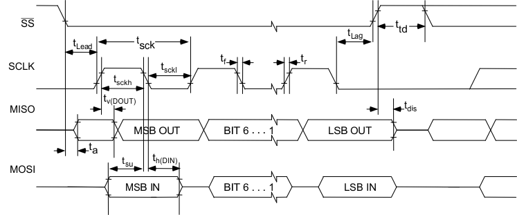 Figure 1. SPI Timing Diagram
 Figure 2. I2S/LJF/RJF Timing in Master Mode
 Figure 3. I2S/LJF/RJF Timing in Slave Mode
 Figure 4. DSP/Mono PCM Timing in Master Mode
 Figure 5. DSP/Mono PCM Timing in Slave Mode
 Figure 6. I2C Interface Timing Diagram
8.19 Typical Characteristics
8.19.1 Audio ADC Performance
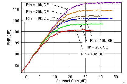 Figure 7. ADC SNR vs Channel Gain Input-Referred
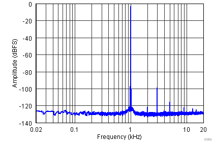 Figure 9. ADC Differential Input to ADC FFT at –3 dBr vs Frequency
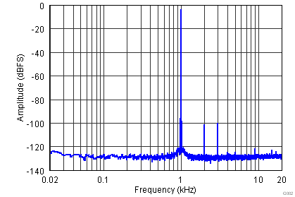 Figure 8. ADC Single-Ended Input to ADC FFT at –3 dBr vs Frequency
8.19.2 Audio DAC Performance
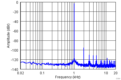 Figure 10. DAC to Line Output FFT Amplitude at –3 dBFS vs Frequency 10-kΩ Load
 Figure 12. DAC to Headphone Output (GCHP) FFT Amplitude at –3 dBFS vs Frequency 32-Ω Load
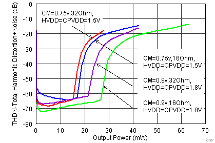 Figure 14. Total Harmonic Distortion + Noise vs Headphone (GCHP) Output Power 9-dB Gain
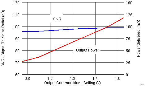 Figure 16. Differential Receiver SNR and Output Power vs Output Common Mode Setting 32-Ω Load
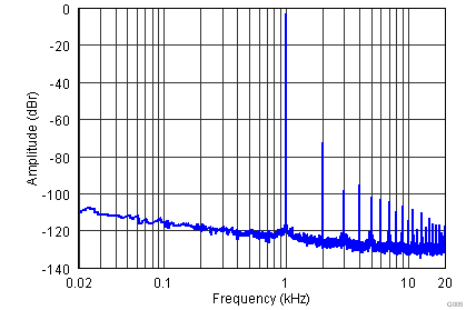 Figure 11. DAC to Headphone Output (GCHP) FFT Amplitude at –3 dBFS vs Frequency 16-Ω Load
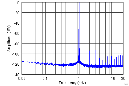 Figure 13. DAC to Differential Receiver Output FFT Amplitude at –3 dBFS vs Frequency 32-Ω Load
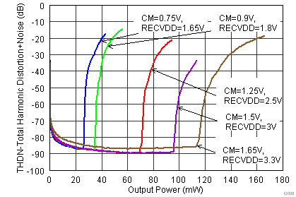 Figure 15. Total Harmonic Distortion + Noise vs Differential Receiver Output Power 32-Ω Load
8.19.3 Class-D Driver Performance
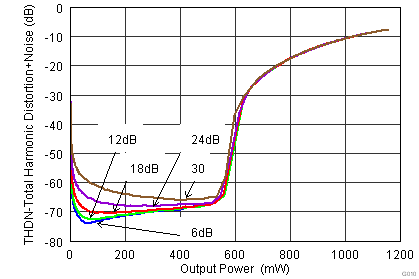 Figure 17. Total Harmonic Distortion + Noise vs Output Power
Different Gain Settings, 8-Ω Load, SLVDD = SRVDD = SPK_V = 3.6 V
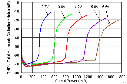 Figure 18. Total Harmonic Distortion + Noise vs Output Power
Different SLVDD/SRVDD/SPK_V Supplies, 8-Ω Load, 12-dB Gain
8.19.4 MICBIAS Performance
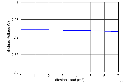 Figure 19. MICBIAS Mode 2, CM = 0.9 V, AVDD3_33 OP STAGE vs Micbias Load Current