SLAS538B October 2007 – November 2016 TLV320AIC34
PRODUCTION DATA.
- 1 Features
- 2 Applications
- 3 Description
- 4 Revision History
- 5 Description (continued)
- 6 Device Comparison Table
- 7 Pin Configuration and Functions
- 8 Specifications
-
9 Detailed Description
- 9.1 Overview
- 9.2 Functional Block Diagram
- 9.3
Feature Description
- 9.3.1 Hardware Reset
- 9.3.2 I2C Bus Debug In A Glitched System
- 9.3.3 Digital Audio Data Serial Interface
- 9.3.4 TDM Data Transfer
- 9.3.5 Audio Data Converters
- 9.3.6 Audio Clock Generation
- 9.3.7 Stereo Audio ADC
- 9.3.8 Digital Audio Processing For Record Path
- 9.3.9 Automatic Gain Control (AGC)
- 9.3.10 Stereo Audio DAC
- 9.3.11 Digital Audio Processing For Playback
- 9.3.12 Digital Interpolation Filter
- 9.3.13 Delta-Sigma Audio DAC
- 9.3.14 Audio DAC Digital Volume Control
- 9.3.15 Increasing DAC Dynamic Range
- 9.3.16 Analog Output Common-Mode Adjustment
- 9.3.17 Audio DAC Power Control
- 9.3.18 Audio Analog Inputs
- 9.3.19 Analog Input Bypass Path Functionality
- 9.3.20 ADC PGA Signal Bypass Path Functionality
- 9.3.21 Input Impedance and VCM Control
- 9.3.22 Passive Analog Bypass During Power Down
- 9.3.23 MICBIAS_x Generation
- 9.3.24 Digital Microphone Connectivity
- 9.3.25 Analog Fully Differential Line Output Drivers
- 9.3.26 Analog High-Power Output Drivers
- 9.3.27 Short-Circuit Output Protection
- 9.3.28 Jack or Headset Detection
- 9.3.29 Output Stage Volume Controls
- 9.4 Device Functional Modes
- 9.5 Programming
- 9.6 Register Maps
- 10Application and Implementation
- 11Power Supply Recommendations
- 12Layout
- 13Device and Documentation Support
- 14Mechanical, Packaging, and Orderable Information
11 Power Supply Recommendations
The TLV320AIC34 device is designed to be extremely tolerant of power supply sequencing. However, in some rare instances, unexpected conditions can be attributed to power supply sequencing. The following sequence provides the most robust operation.
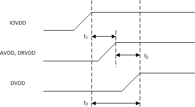
IOVDD must be powered up first. The analog supplies, which include AVDD and DRVDD, must be powered up second. The digital supply DVDD must be powered up last. Keep RESET low until all supplies are stable. The analog supplies must be greater than or equal to DVDD at all times.
 Figure 41. TLV320AIC34 Power Supply Sequencing
Table 10. Power Supply Sequencing
| PARAMETER | MIN | MAX | UNIT | |
|---|---|---|---|---|
| t1 | IOVDD to AVDD, DRVDD | 0 | ms | |
| t2 | AVDD to DVDD | 0 | 5 | ms |
| t3 | IOVDD to DVDD | 0 | ms | |
All power supplies must be stable while the device is in use. Ripples must be avoided if possible because this could affect the device performance. The decoupling capacitors for the power supplies must be placed close to the device terminals.