SLCS135B August 2000 – January 2017 TLV3401 , TLV3402 , TLV3404
PRODUCTION DATA.
- 1 Features
- 2 Applications
- 3 Description
- 4 Revision History
- 5 Device Comparison Table
- 6 Pin Configuration and Functions
- 7 Specifications
- 8 Detailed Description
- 9 Application and Implementation
- 10Power Supply Recommendations
- 11Layout
- 12Device and Documentation Support
- 13Mechanical, Packaging, and Orderable Information
封装选项
机械数据 (封装 | 引脚)
散热焊盘机械数据 (封装 | 引脚)
订购信息
9 Application and Implementation
NOTE
Information in the following applications sections is not part of the TI component specification, and TI does not warrant its accuracy or completeness. TI’s customers are responsible for determining suitability of components for their purposes. Customers should validate and test their design implementation to confirm system functionality.
9.1 Application Information
Many applications require the detection of a signal (voltage or current) that exceeds a particular threshold voltage or current. Using a comparator to make that threshold detection is the easiest, lowest power and highest speed way to make a threshold detection.
9.2 Typical Application
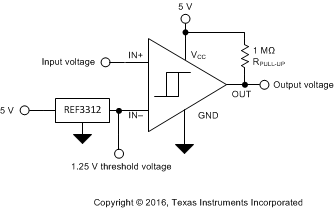
 Figure 16. 1.25-V Threshold Detector
9.2.1 Design Requirements
- Detect when a signal is above or below 1.25 V
- Operate from a single 5-V power supply
- Rail-to-rail input voltage range from 0 to 5 V
- Rail-to-rail output voltage range from 0 to 5 V
9.2.2 Detailed Design Procedure
The input voltage range in the circuit illustrated in Figure 16 is limited only by the power supply applied to the TV3401. In this example with the selection of a 5-V, single-supply power supply, the input voltage range is limited to 0 to VS + 5 V, or 0 to 10 V. The threshold voltage of 1.25 V can de derived in a variety of ways. As the TLV3401 is a very low-power device, it is desirable to also use very low power to create the threshold voltage. The REF3312 series voltage reference is selected for its stable output voltage of 1.25 V and its low power consumption of only 3.9 µA. The TLV3401 is an open-drain output comparator, requiring a pullup resistor from output to the power supply. Proper selection of the pullup resistor value requires maximizing the output voltage swing while at the same time minimizing power dissipated in the resistor when the output voltage is low. Too small of a pullup resistor can result in too much power dissipation, while too large of a pullup resistor can result in slower response times. The TLV3401 is fully specified with a 1-MΩ pullup resistor and using a 1-MΩ pullup resistor results in meeting the performance specifications listed in the Electrical Characteristics.
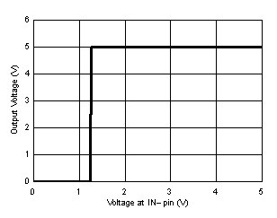
9.2.3 Application Curve
