SLCS135B August 2000 – January 2017 TLV3401 , TLV3402 , TLV3404
PRODUCTION DATA.
- 1 Features
- 2 Applications
- 3 Description
- 4 Revision History
- 5 Device Comparison Table
- 6 Pin Configuration and Functions
- 7 Specifications
- 8 Detailed Description
- 9 Application and Implementation
- 10Power Supply Recommendations
- 11Layout
- 12Device and Documentation Support
- 13Mechanical, Packaging, and Orderable Information
封装选项
机械数据 (封装 | 引脚)
散热焊盘机械数据 (封装 | 引脚)
订购信息
6 Pin Configuration and Functions
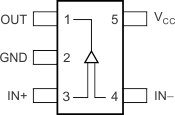
TLV3401: DBV Package
5-Pin SOT-23
Top View

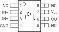
TLV3401: D and P Packages
8-Pin SOIC and VSSOP
Top View

Pin Functions: TLV3401
| PIN | I/O | DESCRIPTION | ||
|---|---|---|---|---|
| NAME | TLV3401 | |||
| SOT-23 | SOIC, PDIP | |||
| GND | 2 | 4 | — | Ground |
| IN– | 4 | 2 | I | Negative (inverting) input |
| IN+ | 3 | 3 | I | Positive (noninverting) input |
| NC | — | 1, 5, 8 | — | No internal connection (can be left floating) |
| OUT | 1 | 6 | O | Output |
| VCC | 5 | 7 | — | Positive power supply |
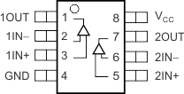
TLV3402: D, DGK, and P Packages
8-PIN SOIC, PDIP, and VSSOP
Top View

Pin Functions: TLV3402
| PIN | I/O | DESCRIPTION | |
|---|---|---|---|
| NAME | TLV3402 | ||
| SOIC, PDIP, VSSOP | |||
| GND | 4 | — | Ground |
| 1IN– | 2 | I | Inverting input, channel 1 |
| 2IN– | 6 | I | Inverting input, channel 2 |
| 1IN+ | 3 | I | Noninverting input, channel 1 |
| 2IN+ | 5 | I | Noninverting input, channel 2 |
| 1OUT | 1 | O | Output, channel 1 |
| 2OUT | 7 | O | Output, channel 2 |
| VCC | 8 | — | Positive power supply |
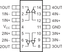
TLV3404: D, N, and PW Packages
14-PIN SOIC, PDIP, TSSOP
Top View

Pin Functions: TLV3404
| PIN | I/O | DESCRIPTION | |
|---|---|---|---|
| NAME | TLV3404 | ||
| SOIC, PDIP, TSSOP | |||
| GND | 11 | — | Ground |
| 1IN– | 2 | I | Inverting input, channel 1 |
| 2IN– | 6 | I | Inverting input, channel 2 |
| 3IN– | 9 | I | Inverting input, channel 3 |
| 4IN– | 13 | I | Inverting input, channel 4 |
| 1IN+ | 3 | I | Noninverting input, channel 1 |
| 2IN+ | 5 | I | Noninverting input, channel 2 |
| 3IN+ | 10 | I | Noninverting input, channel 3 |
| 4IN+ | 12 | I | Noninverting input, channel 4 |
| 1OUT | 1 | O | Output, channel 1 |
| 2OUT | 7 | O | Output, channel 2 |
| 3OUT | 8 | O | Output, channel 3 |
| 4OUT | 14 | O | Output, channel 4 |
| VCC | 4 | — | Positive power supply |