SBOS262E December 2002 – December 2016 TLV3491 , TLV3492 , TLV3494
PRODUCTION DATA.
- 1 Features
- 2 Applications
- 3 Description
- 4 Revision History
- 5 Device Comparison Table
- 6 Pin Configuration and Functions
- 7 Specifications
- 8 Detailed Description
- 9 Application and Implementation
- 10Power Supply Recommendations
- 11Layout
- 12Device and Documentation Support
- 13Mechanical, Packaging, and Orderable Information
封装选项
机械数据 (封装 | 引脚)
散热焊盘机械数据 (封装 | 引脚)
- DCN|8
订购信息
9 Application and Implementation
NOTE
Information in the following applications sections is not part of the TI component specification, and TI does not warrant its accuracy or completeness. TI’s customers are responsible for determining suitability of components for their purposes. Customers should validate and test their design implementation to confirm system functionality.
9.1 Application Information
The TLV349x family of comparators features rail-to-rail input and output on supply voltages as low as 1.8 V. The push-pull output stage is optimal for reduced power budget applications and features no shoot-through current. Low supply voltages, common-mode input range beyond supply rails, and a typical supply current of 0.8 µA make the TLV349x family an excellent candidate for battery-powered applications with single-cell operation.
9.2 Typical Applications
9.2.1 TLV3491 Configured as an AC-Coupled Comparator
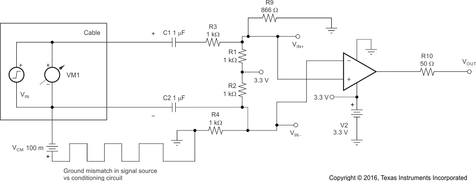
One of the benefits of AC coupling a single-supply comparator circuit is that it can block dc offsets induced by ground-loop offsets that could potentially produce either a false trip or a common-mode input violation. Figure 18 shows the TLV3491 configured as an AC-coupled comparator.
 Figure 18. TLV3491 Configured as an AC-Coupled Comparator (Schematic)
9.2.1.1 Design Requirements
Design requirements include:
- Ability to tolerate up to ±100 mV of common-mode signal.
- Trigger only on AC signals (such as zero-cross detection).
9.2.1.2 Detailed Design Procedure
Design analysis:
- AC-coupled, high-pass frequency
- Large capacitors require longer start-up time from device power on
- Use 1-µF capacitor to achieve high-pass frequency of approximately 159 Hz
- For high-pass equivalent, use CIN = 0.5 µF, RIN = 2 kΩ
- Set up input dividers initially for one-half supply (to be in center of acceptable common-mode range).
- Adjust either divider slightly upwards or downwards as desired to establish quiescent output condition.
- Select coupling capacitors based on lowest expected frequency.
9.2.1.3 Application Curve
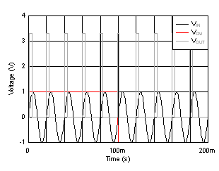
 Figure 19. AC-Coupled Comparator Results
9.2.2 Relaxation Oscillator
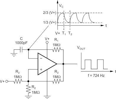
The TLV349x can be configured as a relaxation oscillator to provide a simple and inexpensive clock output, as Figure 20 shows. The capacitor is charged at a rate of 0.69 RC. It also discharges at a rate of 0.69RC. Therefore, the period is 1.38 RC. R1 may be a different value than R2.
 Figure 20. TLV349x Configured as a Relaxation Oscillator
9.2.3 Power-On Reset
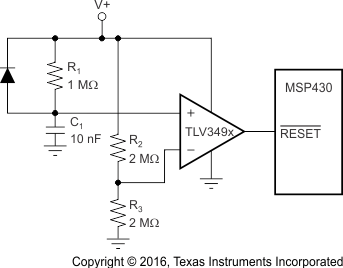
The reset circuit shown in Figure 21 provides a time-delayed release of reset to the MSP430 microcontroller. Operation of the circuit is based on a stabilization time constant of the supply voltage, rather than on a predetermined voltage value. The negative input is a reference voltage created by a simple resistor divider.
These resistor values must be relatively high to reduce the current consumption of the circuit. The positive input is an RC circuit that provides a power-up delay. When power is applied, the output of the comparator is low, holding the processor in the reset condition. Only after allowing time for the supply voltage to stabilize does the positive input of the comparator become higher than the negative input, resulting in a high output state and releasing the processor for operation. The stabilization time required for the supply voltage is adjustable by the selection of the RC component values.
Use of a lower-valued resistor in this portion of the circuit does not increase current consumption because no current flows through the RC circuit after the supply has stabilized. The required reset delay time depends on the power-up characteristics of the system power supply. R1 and C1 are selected to allow enough time for the power supply to stabilize. D1 provides rapid reset if power is lost. In this example, the R1 × C1 time constant is 10 ms.
 Figure 21. The TLV349x Configured as a Reset Circuit for the MSP430