SBOS262E December 2002 – December 2016 TLV3491 , TLV3492 , TLV3494
PRODUCTION DATA.
- 1 Features
- 2 Applications
- 3 Description
- 4 Revision History
- 5 Device Comparison Table
- 6 Pin Configuration and Functions
- 7 Specifications
- 8 Detailed Description
- 9 Application and Implementation
- 10Power Supply Recommendations
- 11Layout
- 12Device and Documentation Support
- 13Mechanical, Packaging, and Orderable Information
封装选项
机械数据 (封装 | 引脚)
散热焊盘机械数据 (封装 | 引脚)
- DCN|8
订购信息
8 Detailed Description
8.1 Overview
The TLV349x family of comparators features rail-to-rail input and output on supply voltages as low as 1.8 V. The push-pull output stage is optimal for reduced power budget applications and features no shoot-through current. Low supply voltages, common-mode input range beyond supply rails, and a typical supply current of 0.8 µA make the TLV349x family an excellent candidate for battery-powered applications with single-cell operation as well as a wide range of low-voltage applications. The devices are available in a selection of micro-sized packages for space-constrained and portable applications.
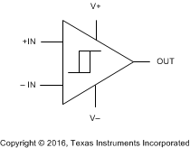
8.2 Functional Block Diagram

8.3 Feature Description
8.3.1 Operating Voltage
The TLV349x comparators are specified for use on a single supply from 1.8 V to 5.5 V (or a dual supply from ±0.9 V to ±2.75 V) over a temperature range of −40°C to 125°C.
8.3.2 Input Overvoltage Protection
The device inputs are protected by electrostatic discharge (ESD) diodes that conduct if the input voltages exceed the power supplies by more than approximately 500 mV. Momentary voltages greater than 500 mV beyond the power supply can be tolerated if the input current is limited to 10 mA. This limiting is easily accomplished with a small input resistor in series with the input to the comparator.
8.3.3 Setting Reference Voltage
It is important to use a stable reference when setting the transition point for the TLV349x. The REF1004 provides a 1.25-V reference voltage with low drift and only 8 µA of quiescent current.
8.3.4 External Hysteresis
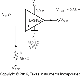
Comparator inputs have no noise immunity within the range of specified offset voltage (±15 mV). For noisy input signals, the comparator output typically displays multiple switching as input signals move through the switching threshold. The typical comparator threshold of the TLV349x is ±15 mV. To prevent multiple switching within the comparator threshold of the TLV349x, external hysteresis must be added by connecting a small amount of feedback to the positive input. Figure 17 shows a typical topology used to introduce hysteresis, described in Equation 1.

VHYST sets the value of the transition voltage required to switch the comparator output by increasing the threshold region, thereby reducing sensitivity to noise.
 Figure 17. Adding Hysteresis to the TLV349x
8.4 Device Functional Modes
The TLV349x has a single functional mode and is operational when the power-supply voltage is between 1.8 V and 5.5 V.