SBOS262E December 2002 – December 2016 TLV3491 , TLV3492 , TLV3494
PRODUCTION DATA.
- 1 Features
- 2 Applications
- 3 Description
- 4 Revision History
- 5 Device Comparison Table
- 6 Pin Configuration and Functions
- 7 Specifications
- 8 Detailed Description
- 9 Application and Implementation
- 10Power Supply Recommendations
- 11Layout
- 12Device and Documentation Support
- 13Mechanical, Packaging, and Orderable Information
封装选项
机械数据 (封装 | 引脚)
散热焊盘机械数据 (封装 | 引脚)
- DCN|8
订购信息
11 Layout
11.1 Layout Guidelines
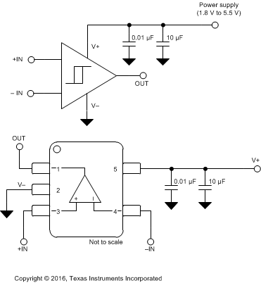
Figure 22 shows the typical connections for the TLV349x. To minimize supply noise, power supplies must be capacitively decoupled by a 0.01-µF ceramic capacitor in parallel with a 10-µF electrolytic capacitor. Comparators are very sensitive to input noise. Proper grounding (the use of a ground plane) helps to maintain the specified performance of the TLV349x family.
For best results, maintain the following layout guidelines:
- Use a printed-circuit board (PCB) with a good, unbroken low-inductance ground plane.
- Place a decoupling capacitor (0.1-µF ceramic, surface-mount capacitor) as close as possible to VCC.
- On the inputs and the output, keep lead lengths as short as possible to avoid unwanted parasitic feedback around the comparator. Keep inputs away from the output.
- Solder the device directly to the PCB rather than using a socket.
- For slow-moving input signals, take care to prevent parasitic feedback. A small capacitor (1000 pF or less) placed between the inputs can help eliminate oscillations in the transition region. This capacitor causes some degradation to propagation delay when the impedance is low. The topside ground plane runs between the output and inputs.
- The ground pin ground trace runs under the device up to the bypass capacitor, shielding the inputs from the outputs.
11.2 Layout Example
 Figure 22. Basic Connections of the TLV349x