SBOS321E March 2005 – April 2016 TLV3501 , TLV3502
PRODUCTION DATA.
- 1 Features
- 2 Applications
- 3 Description
- 4 Revision History
- 5 Pin Configuration and Functions
- 6 Specifications
- 7 Detailed Description
- 8 Application and Implementation
- 9 Power Supply Recommendations
- 10Layout
- 11Device and Documentation Support
- 12Mechanical, Packaging, and Orderable Information
封装选项
机械数据 (封装 | 引脚)
散热焊盘机械数据 (封装 | 引脚)
- DCN|8
订购信息
7 Detailed Description
7.1 Overview
The TLV3501 and TLV3502 devices both feature high-speed response and include 6 mV of internal hysteresis for improved noise immunity with an input common-mode range that extends 0.2 V beyond the power-supply rails.
7.2 Functional Block Diagram

7.3 Feature Description
7.3.1 Operating Voltage
The TLV350x comparators are specified for use on a single supply from 2.7 V to 5.5 V (or a dual supply from ±1.35 V to ±2.75 V) over a temperature range of −40°C to +125°C. These devices continue to function below this range, but performance is not specified.
7.3.2 Input Overvoltage Protection
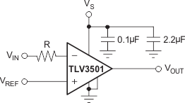
Device inputs are protected by electrostatic discharge (ESD) diodes that conduct if the input voltages exceed the power supplies by more than approximately 300 mV. Momentary voltages greater than 300 mV beyond the power supply can be tolerated if the input current is limited to 10 mA. This limiting is easily accomplished with a small input resistor in series with the comparator, as shown in Figure 15.
 Figure 15. Input Current Protection for Voltages Exceeding the Supply Voltage
7.4 Device Functional Modes
7.4.1 Shutdown
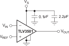
A shutdown pin allows the device to go into idle when it is not in use. When the shutdown pin is high, the device draws approximately 2 μA, and the output goes to high impedance. When the shutdown pin is low, the TLV3501 is active. When the TLV3501 shutdown feature is not used, connect the shutdown pin to the most negative supply, as shown in Figure 16. Exiting shutdown mode requires approximately 100 ns. The TLV3502 does not have the shutdown feature.
 Figure 16. Basic Connections for the TLV3501