ZHCSF19 May 2016 TLV2369 , TLV369
PRODUCTION DATA.
8 Application and Implementation
NOTE
Information in the following applications sections is not part of the TI component specification, and TI does not warrant its accuracy or completeness. TI’s customers are responsible for determining suitability of components for their purposes. Customers should validate and test their design implementation to confirm system functionality.
8.1 Application Information
When designing for ultra-low power, choose system components carefully. To minimize current consumption, select large-value resistors. Any resistors can react with stray capacitance in the circuit and the input capacitance of the operational amplifier. These parasitic RC combinations can affect the stability of the overall system. Use of a feedback capacitor assures stability and limits overshoot or gain peaking.
8.2 Typical Application
A typical application for an operational amplifier is an inverting amplifier, as shown in Figure 15. An inverting amplifier takes a positive voltage on the input and outputs a signal inverted to the input, making a negative voltage of the same magnitude. In the same manner, the amplifier also makes negative input voltages positive on the output. In addition, amplification can be added by selecting the input resistor RI and the feedback resistor RF.
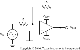 Figure 15. Application Schematic
8.2.1 Design Requirements
The supply voltage must be chosen to be larger than the input voltage range and the desired output range. The limits of the input common-mode range (VCM) and the output voltage swing to the rails (VO) must also be considered. For instance, this application scales a signal of ±0.5 V (1 V) to ±1.8 V (3.6 V). Setting the supply at ±2.5 V is sufficient to accommodate this application.
8.2.2 Detailed Design Procedure
Determine the gain required by the inverting amplifier using Equation 1 and Equation 2:


When the desired gain is determined, choose a value for RI or RF. Choosing a value in the kilohm range is desirable for general-purpose applications because the amplifier circuit uses currents in the milliamp range. This milliamp current range ensures that the device does not draw too much current. The trade-off is that very large resistors (100s of kilohms) draw the smallest current but generate the highest noise. Very small resistors (100s of ohms) generate low noise but draw high current. This example uses 10 kΩ for RI, meaning 36 kΩ is used for RF. These values are determined by Equation 3:

8.2.3 Application Curve
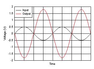 Figure 16. Inverting Amplifier Input and Output
8.3 System Examples
8.3.1 Battery Monitoring
The low operating voltage and quiescent current of the TLV369 series make the family an excellent choice for battery-monitoring applications, as shown in Figure 17.
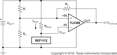 Figure 17. Battery Monitor
In this circuit, VSTATUS is high as long as the battery voltage remains above 2 V. A low-power reference is used to set the trip point. Resistor values are selected as follows:
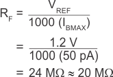
- Selecting RF: Select RF such that the current through RF is approximately 1000 times larger than the maximum bias current over temperature, as given by Equation 4:
- Choose the hysteresis voltage, VHYST. For battery-monitoring applications, 50 mV is adequate.
- Calculate R1 as calculated by Equation 5:
- Select a threshold voltage for VIN rising (VTHRS) = 2.0 V.
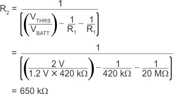
- Calculate R2 as given by Equation 6:
- Calculate RBIAS: The minimum supply voltage for this circuit is 1.8 V. The REF1112 has a current requirement of 1.2 μA (max). Providing the REF1112 with 2 μA of supply current assures proper operation. Therefore, RBIAS is as given by Equation 7.


8.3.2 Window Comparator
Figure 18 shows the TLV2369 used as a window comparator. The threshold limits are set by VH and VL, with VH greater than VL. When VIN is less than VH, the output of A1 is low. When VIN is greater than VL, the output of A2 is low. Therefore, both op amp outputs are at 0 V as long as VIN is between VH and VL. This architecture results in no current flowing through either diode, Q1 is in cutoff, with the base voltage at 0 V, and VOUT forced high.
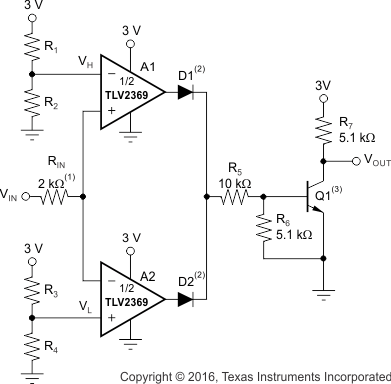 Figure 18. TLV2369 as a Window Comparator
If VIN falls below VL, the output of A2 is high, current flows through D2, and VOUT is low. Likewise, if VIN rises above VH, the output of A1 is high, current flows through D1, and VOUT is low. The window comparator threshold voltages are set as shown by Equation 8 and Equation 9:

