ZHCSBY0A December 2013 – November 2015 TLV3691
PRODUCTION DATA.
8 Application and Implementation
NOTE
Information in the following applications sections is not part of the TI component specification, and TI does not warrant its accuracy or completeness. TI’s customers are responsible for determining suitability of components for their purposes. Customers should validate and test their design implementation to confirm system functionality.
8.1 Application Information
The TLV3691 comparators feature rail-to-rail inputs and outputs on supply voltages as low as 0.9 V. The push-pull output stage is optimal for reduced power budget applications and features no shoot-through current. Low minimum supply voltages, common-mode input range beyond supply rails, and a typical supply current of 75 nA make the TLV3691 an excellent candidate for battery-operated and portable, handheld designs.
8.1.1 Comparator Inputs
The TLV3691 is a rail-to-rail input comparator, with an input common-mode range that exceeds the supply rails by 100 mV for both positive and negative supplies. The device is designed to prevent phase inversion when the input pins exceed the supply voltage. Figure 27 shows the device response when input voltages exceed the supply, resulting in no phase inversion.
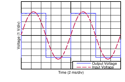 Figure 27. No Phase Inversion: Comparator Response to Input Voltage (Propagation Delay Included)
8.1.2 External Hysteresis
The device hysteresis transfer curve is shown in Figure 28. This curve is a function of three components: VTH, VOS, and VHYST.
- VTH is the actual set voltage or threshold trip voltage.
- VOS is the internal offset voltage between VIN+ and VIN–. This voltage is added to VTH to form the actual trip point at which the comparator must respond to change output states.
- VHYST is the internal hysteresis (or trip window) that is designed to reduce comparator sensitivity to noise
(17 mV for the TLV3691).
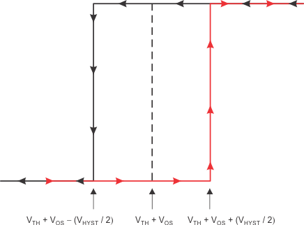 Figure 28. Hysteresis Transfer Curve
8.1.2.1 Inverting Comparator With Hysteresis
The inverting comparator with hysteresis requires a three-resistor network that is referenced to the comparator supply voltage (VCC), as shown in Figure 29. When VIN at the inverting input is less than VA, the output voltage is high (for simplicity, assume VO switches as high as VCC). The three network resistors can be represented as R1 || R3 in series with R2. Equation 1 defines the high-to-low trip voltage (VA1).

When VIN is greater than VA, the output voltage is low, very close to ground. In this case, the three network resistors can be presented as R2 || R3 in series with R1. Use Equation 2 to define the low to high trip voltage (VA2).

Equation 3 defines the total hysteresis provided by the network.

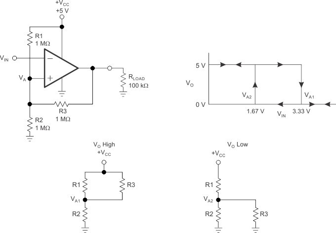 Figure 29. TLV3691 in an Inverting Configuration With Hysteresis
8.1.2.2 Noninverting Comparator With Hysteresis
A noninverting comparator with hysteresis requires a two-resistor network, as shown in Figure 30, and a voltage reference (VREF) at the inverting input. When VIN is low, the output is also low. For the output to switch from low to high, VIN must rise to VIN1. Use Equation 4 to calculate VIN1.

When VIN is high, the output is also high. For the comparator to switch back to a low state, VIN must drop to VIN2 such that VA is equal to VREF. Use Equation 5 to calculate VIN2.

The hysteresis of this circuit is the difference between VIN1 and VIN2, as shown in Equation 6.

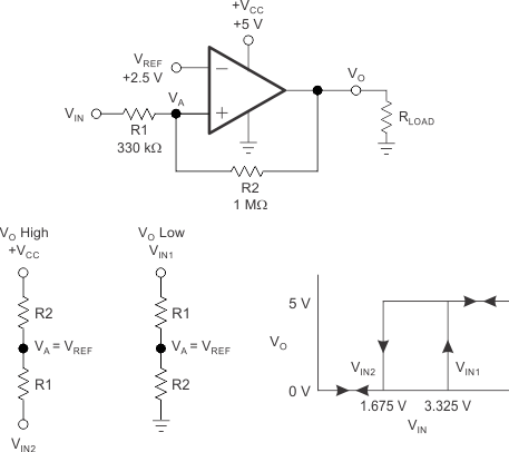 Figure 30. TLV3691 in a Noninverting Configuration With Hysteresis
8.1.3 Capacitive Loads
Under reasonable capacitive loads, the device maintains specified propagation delay (see Typical Characteristics). However, excessive capacitive loading under high switching frequencies may increase supply current, propagation delay, or induce decreased slew rate.
8.2 Typical Application
8.2.1 Window Comparator
Window comparators are commonly used to detect undervoltage and overvoltage conditions. Figure 32 illustrates a simple window comparator circuit.
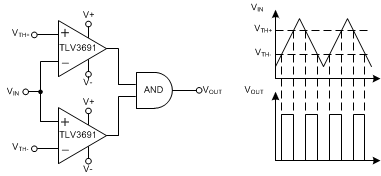 Figure 32. Window Comparator
8.2.1.1 Design Requirements
- Alert when an input signal is less than 1.25 V
- Alert when an input signal is greater than 3.3 V
- Alert signal is active low
- Operate from 5-V power supply
- Consume less than 1 µA over the temperature range from –40°C to 125°C
8.2.1.2 Detailed Design Procedure
Configure the circuit as shown in Figure 32. Connect V+ to a 5-V power supply. Connect V- to ground. Connect VTH- to a 1.25-V voltage source; this can be a low power voltage reference such as REF3312. Connect VTH+ to a 3.3-V voltage source; this can be a low power voltage reference such as REF3333. Apply an input voltage at VIN. VOUT will be low when VIN is less than 1.25 V or greater than 3.3 V. VOUT will be high when VIN is in the range of 1.25 V to 3.3 V.
8.2.1.3 Application Curve
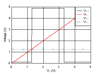 Figure 33. Window Comparator Results
8.2.2 Overvoltage and Undervoltage Detection
The TLV3691 can be easily configured as and overvoltage and undervoltage detection circuit. Figure 34 illustrates an overvoltage and undervoltage detection circuit. This circuit can be configured to detect the validity of a bus voltage source. The outputs of the TLV3691 will transition low when the bus voltage is out of range.
- A bus voltage overvoltage condition is indicated when VOV is low. VOV will transition low according to Equation 7.
- A bus voltage undervoltage condition is indicated when VUV is low. VUV will transition low according to Equation 8.
- VOV and VUV will both be high when the bus voltage is within the desired range determined by Equation 7 and Equation 8.


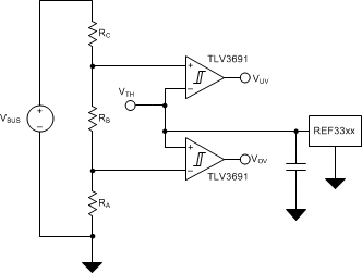 Figure 34. Overvoltage and Undervoltage Detection
