SLCS137D November 2000 – May 2017 TLV3701 , TLV3702 , TLV3704
PRODUCTION DATA.
- 1 Features
- 2 Applications
- 3 Description
- 4 Revision History
- 5 Device Comparison Tables
- 6 Pin Configuration and Functions
- 7 Specifications
- 8 Detailed Description
- 9 Application and Implementation
- 10Power Supply Recommendations
- 11Layout
- 12Device and Documentation Support
- 13Mechanical, Packaging, and Orderable Information
封装选项
机械数据 (封装 | 引脚)
散热焊盘机械数据 (封装 | 引脚)
订购信息
7 Specifications
7.1 Absolute Maximum Ratings
over operating free-air temperature range (unless otherwise noted)(1)| MIN | MAX | UNIT | ||
|---|---|---|---|---|
| Supply voltage, VCC(2) | 17 | V | ||
| Differential input voltage, VID | ±20 | V | ||
| Input voltage, VI(2)(3) | 0 | VCC + 5 | V | |
| Input current, II | ±10 | mA | ||
| Output current, IO | ±10 | mA | ||
| Continuous total power dissipation | See Dissipation Ratings | |||
| Maximum junction temperature, TJ | 150 | °C | ||
| Lead temperature 1,6 mm (1/16 inch) from case for 10 seconds | 260 | °C | ||
| Storage temperature, Tstg | –65 | 150 | °C | |
(1) Stresses beyond those listed under Absolute Maximum Ratings may cause permanent damage to the device. These are stress ratings only, which do not imply functional operation of the device at these or any other conditions beyond those indicated under Recommended Operating Conditions. Exposure to absolute-maximum-rated conditions for extended periods may affect device reliability.
(2) All voltage values, except differential voltages, are with respect to GND.
(3) Input voltage range is limited to 20 V maximum or VCC + 5 V, whichever is smaller.
7.2 Recommended Operating Conditions
over operating free-air temperature range (unless otherwise noted)| MIN | MAX | UNIT | |||
|---|---|---|---|---|---|
| Supply voltage, VCC | Single supply | C-suffix | 2.5 | 16 | V |
| I-suffix | 2.7 | 16 | |||
| Split supply | C-suffix | ±1.25 | ±8 | ||
| I-suffix | ±1.35 | ±8 | |||
| Common-mode input voltage, VICR | –0.1 | VCC + 5 | V | ||
| Operating free-air temperature, TA | C-suffix | 0 | 70 | °C | |
| I-suffix | –40 | 125 | |||
7.3 Thermal Information – TLV3701
| THERMAL METRIC(1) | TLV3701 | UNIT | |||
|---|---|---|---|---|---|
| DBV (SOT-23) | D (SOIC) | P (PDIP) | |||
| 5 PINS | 8 PINS | ||||
| RθJA | Junction-to-ambient thermal resistance | 193.6 | 124.8 | 82.8 | °C/W |
| RθJC(top) | Junction-to-case (top) thermal resistance | 102.4 | 69.1 | 84.8 | °C/W |
| RθJB | Junction-to-board thermal resistance | 54.3 | 67.9 | 59.7 | °C/W |
| ψJT | Junction-to-top characterization parameter | 16.9 | 22.3 | 45.3 | °C/W |
| ψJB | Junction-to-board characterization parameter | 53.6 | 67.2 | 59.5 | °C/W |
| RθJC(bot) | Junction-to-case (bottom) thermal resistance | — | — | — | °C/W |
(1) For more information about traditional and new thermal metrics, see the Semiconductor and IC Package Thermal Metrics application report.
7.4 Thermal Information – TLV3702
| THERMAL METRIC(1) | TLV3702 | UNIT | |||
|---|---|---|---|---|---|
| D (SOIC) | DGK (VSSOP) | P (PDIP) | |||
| 8 PINS | |||||
| RθJA | Junction-to-ambient thermal resistance | 116.7 | 163.9 | 77.1 | °C/W |
| RθJC(top) | Junction-to-case (top) thermal resistance | 59.4 | 65.7 | 79 | °C/W |
| RθJB | Junction-to-board thermal resistance | 60.2 | 85.3 | 54 | °C/W |
| ψJT | Junction-to-top characterization parameter | 14.6 | 9 | 39.5 | °C/W |
| ψJB | Junction-to-board characterization parameter | 59.5 | 83.9 | 53.7 | °C/W |
| RθJC(bot) | Junction-to-case (bottom) thermal resistance | — | — | — | °C/W |
(1) For more information about traditional and new thermal metrics, see the Semiconductor and IC Package Thermal Metrics application report.
7.5 Thermal Information – TLV3704
| THERMAL METRIC(1) | TLV3704 | UNIT | |||
|---|---|---|---|---|---|
| D (SOIC) | N (PDIP) | PW (TSSOP) | |||
| 14 PINS | |||||
| RθJA | Junction-to-ambient thermal resistance | 81.4 | 58.1 | 105.7 | °C/W |
| RθJC(top) | Junction-to-case (top) thermal resistance | 38.1 | 50.9 | 33.9 | °C/W |
| RθJB | Junction-to-board thermal resistance | 37.8 | 38 | 49.5 | °C/W |
| ψJT | Junction-to-top characterization parameter | 7.5 | 23.6 | 2.5 | °C/W |
| ψJB | Junction-to-board characterization parameter | 37.4 | 37.7 | 48.8 | °C/W |
| RθJC(bot) | Junction-to-case (bottom) thermal resistance | — | — | — | °C/W |
(1) For more information about traditional and new thermal metrics, see the Semiconductor and IC Package Thermal Metrics application report.
7.6 Electrical Characteristics
At specified operating free-air temperature range, VCC = 2.7 V, 5 V, 15 V (unless otherwise noted).| PARAMETER | TEST CONDITIONS | TA(1) | MIN | TYP | MAX | UNIT | ||
|---|---|---|---|---|---|---|---|---|
| DC PERFORMANCE | ||||||||
| VIO | Input offset voltage | VIC = VCC/2, RS = 50 Ω | 25°C | 250 | 5000 | µV | ||
| Full range | 7000 | |||||||
| αVIO | Offset voltage drift | VIC = VCC/2, RS = 50 Ω | 25°C | 3 | µV/°C | |||
| CMRR | Common-mode rejection ratio | VIC = 0 to 2.7 V, RS = 50 Ω | 25°C | 55 | 72 | dB | ||
| Full range | 50 | |||||||
| VIC = 0 to 5 V, RS = 50 Ω | 25°C | 60 | 76 | |||||
| Full range | 55 | |||||||
| VIC = 0 to 15 V, RS = 50 Ω | 25°C | 65 | 88 | |||||
| Full range | 60 | |||||||
| AVD | Large-signal differential voltage amplification | 25°C | 1000 | V/mV | ||||
| INPUT/OUTPUT CHARACTERISTICS | ||||||||
| IIO | Input offset current | VIC = VCC/2, RS = 50 Ω | 25°C | 20 | 100 | pA | ||
| Full range | 1000 | |||||||
| IIB | Input bias current | VIC = VCC/2, RS = 50 Ω | 25°C | 80 | 250 | pA | ||
| Full range | 1500 | |||||||
| ri(d) | Differential input resistance | 25°C | 300 | MΩ | ||||
| VOH | High-level output voltage | VIC = VCC/2, IOH = 2 μA, VID = 1 V | 25°C | VCC – 80 | mV | |||
| VIC = VCC/2, IOH = – 50 μA, VID = 1 V | 25°C | VCC – 320 | ||||||
| Full range | VCC – 450 | |||||||
| VOL | Low-level output voltage | VIC = VCC/2, IOH = 2 μA, VID = – 1 V | 25°C | 8 | mV | |||
| VIC = VCC/2, IOH = 50 μA, VID = – 1 V | 25°C | 80 | 200 | |||||
| Full range | 300 | |||||||
| POWER SUPPLY | ||||||||
| ICC | Supply current (per channel) | Output state high | 25°C | 560 | 800 | nA | ||
| Full range | 1000 | |||||||
| PSRR | Power supply rejection ratio | VIC = VCC/2 V, No load | VCC = 2.7 V to 5 V | 25°C | 75 | 100 | dB | |
| Full range | 70 | |||||||
| VCC = 5 V to 15 V | 25°C | 85 | 105 | |||||
| Full range | 80 | |||||||
(1) Full range is 0°C to 70°C for C suffix and –40°C to 125°C for I suffix. If not specified, full range is –40°C to 125°C.
7.7 Switching Characteristics
At specified operating free-air temperature range, VCC = 2.7 V, 5 V, 15 V (unless otherwise noted).| PARAMETER | TEST CONDITIONS | MIN | TYP | MAX | UNIT | ||
|---|---|---|---|---|---|---|---|
| t(PLH) | Propagation response time, low-to-high-level output(1) | f = 10 kHz, VSTEP = 100 mV, CL = 10 pF, VCC = 2.7 V | Overdrive = 2 mV | 240 | µs | ||
| Overdrive = 10 mV | 64 | ||||||
| Overdrive = 50 mV | 36 | ||||||
| t(PHL) | Propagation response time, high-to-low-level output(1) | f = 10 kHz, VSTEP = 100 mV, CL = 10 pF, VCC = 2.7 V | Overdrive = 2 mV | 167 | µs | ||
| Overdrive = 10 mV | 67 | ||||||
| Overdrive = 50 mV | 37 | ||||||
| tr | Rise time | CL = 10 pF, VCC = 2.7 V | 7 | µs | |||
| tf | Fall time | CL = 10 pF, VCC = 2.7 V | 9 | µs | |||
| tsu | Start-up time (TLV3701 Only) | VCC = 2.7 to 15V(2) | 25°C | 7 | 15 | ms | |
| Full range | 14 | 30 | |||||
(1) The response time specified is the interval between the input step function and the instant when the output crosses 1.4 V. Propagation responses are longer at higher supply voltages, refer to Figures 12 – 17 for further details.
7.8 Dissipation Ratings
| PACKAGE | θJC (°C/W) | θJA (°C/W) | TA ≤ 25°C POWER RATING | TA = 125°C POWER RATING |
|---|---|---|---|---|
| D (8) | 69.1 | 124.8 | 1001 mW | 200 mW |
| D (14) | 38.1 | 81.4 | 1536 mW | 307 mW |
| DBV (5) | 102.4 | 193.6 | 646 mW | 129 mW |
| DGK (8) | 65.7 | 163.9 | 763 mW | 153 mW |
| N (14) | 50.9 | 58.1 | 2151 mW | 430 mW |
| P (8) | 84.8 | 82.8 | 1510 mW | 302 mW |
| PW (14) | 33.9 | 105.7 | 1183 mW | 237 mW |
7.9 Typical Characteristics
At specified operating conditions (unless otherwise noted).Table 5. Table of Graphs
| FIGURE | |||
|---|---|---|---|
| Input bias/offset current | vs Free-air temperature | Figure 2 | |
| VOL | Low-level output voltage | vs Low-level output current | Figure 6, Figure 8, Figure 4 |
| VOH | High-level output voltage | vs High-level output current | Figure 3, Figure 5, Figure 7 |
| ICC | Supply current | vs Supply voltage | Figure 1 |
| Free-air temperature | Figure 9 | ||
| Output fall time/rise time | vs Supply voltage | Figure 10 | |
| Low-to-high level output response for various input overdrives | Figure 11, Figure 13, Figure 15 | ||
| High-to-low level output response for various input overdrives | Figure 12, Figure 14, Figure 16 | ||
 Figure 3. High-Level Output Voltage vs High-Level Output Current
 Figure 5. High-Level Output Voltage vs High-Level Output Current
 Figure 7. High-Level Output Voltage vs High-Level Output Current
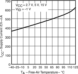 Figure 9. Supply Current vs Free-Air Temperature
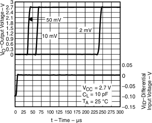 Figure 11. Low-to-High Output Response for Various Input Overdrives
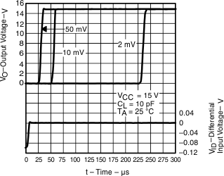 Figure 13. Low-to-High Level Output Response for Various Input Overdrives
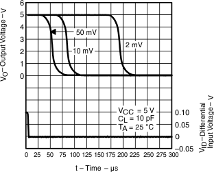 Figure 15. Low-to-High Level Output Response for Various Input Overdrives
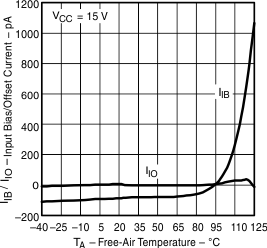 Figure 2. Input Bias/Offset Current vs Free-Air Temperature
 Figure 4. Low-Level Output Voltage vs Low-Level Output Current
 Figure 6. Low-Level Output Voltage vs Low-Level Output Current
 Figure 8. Low-Level Output Voltage vs Low-Level Output Current
 Figure 10. Output Rise/Fall Time vs Supply Voltage
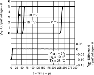 Figure 12. High-to-Low Level Output Response for Various Input Overdrives
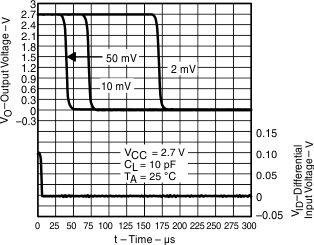 Figure 14. High-to-Low Level Output Response for Various Input Overdrives
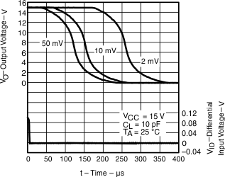 Figure 16. High-to-Low Level Output Response for Various Input Overdrives
