ZHCSIW5C March 2019 – December 2021 TLV4021 , TLV4031 , TLV4041 , TLV4051
PRODUCTION DATA
- 1 特性
- 2 应用
- 3 说明
- 4 Revision History
- 5 Pin Configuration and Functions
- 6 Specifications
- 7 Typical Characteristics
- 8 Detailed Description
- 9 Application and Implementation
- 10Power Supply Recommendations
- 11Layout
- 12Device and Documentation Support
- 13Mechanical, Packaging, and Orderable Information
8.4.1 Power ON Reset (POR)
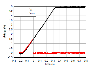
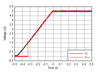
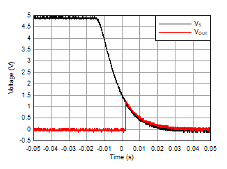
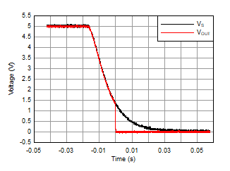
The TLV40x1 comparators have a Power-on-Reset (POR) circuit which provides system designers a known start-up condition for the output of the comparators. When the power supply (VS) is ramping up or ramping down, the POR circuit will be active when VS is below VPOR. For the TLV4021 and TLV4031, the POR circuit will force the output to High-Z, and for the TLV4041 and TLV4051, the POR circuit will hold the output low at (V-). When VS is greater than, or equal to, the minimum recommended operating voltage, the comparator output reflects the state of the input (IN).
The following pictures represent how the TLV40x1 outputs respond for VS rising and falling. For the comparators with open-drain outputs (TLV4021/4031), IN is connected to (V-) to highlight the transition from POR circuit control to standard comparator operation where the output reflects the input condition. Note how the output goes low when VS reaches 1.45V. Likewise, for the comparators with push-pull outputs (TLV4041/4051), the input is connected to (V+). Note how the output goes high when VS reaches 1.45V.
 Figure 8-1 TLV4021/4031 Output for VS Rising
 Figure 8-3 TLV4041/4051 Output for VS Rising
 Figure 8-2 TLV4021/4031 Output for VS Falling
 Figure 8-4 TLV4041/4051 Output for VS Falling