SBVS404A April   2020  – June 2020 TLV4062 , TLV4082

PRODUCTION DATA.  

  1. Features
  2. Applications
  3. Description
    1.     Device Images
      1.      Block Diagram for TLV4062
      2.      Block Diagram for TLV4082
  4. Revision History
  5. Pin Configuration and Functions
    1.     Pin Functions
  6. Specifications
    1. 6.1 Absolute Maximum Ratings
    2. 6.2 ESD Ratings
    3. 6.3 Recommended Operating Conditions
    4. 6.4 Thermal Information
    5. 6.5 Electrical Characteristics
    6. 6.6 Timing Requirements
    7. 6.7 Typical Characteristics
  7. Detailed Description
    1. 7.1 Overview
    2. 7.2 Functional Block Diagrams
    3. 7.3 Feature Description
    4. 7.4 Device Functional Modes
      1. 7.4.1 Inputs (IN1, IN2)
      2. 7.4.2 Outputs (OUT1, OUT2)
      3. 7.4.3 Switching Threshold and Hysteresis
  8. Application and Implementation
    1. 8.1 Application Information
      1. 8.1.1 Threshold Overdrive
    2. 8.2 Typical Applications
      1. 8.2.1 Monitoring Two Separate Rails
        1. 8.2.1.1 Design Requirements
        2. 8.2.1.2 Detailed Design Procedure
        3. 8.2.1.3 Application Curve
      2. 8.2.2 Early Warning Detection
        1. 8.2.2.1 Design Requirements
        2. 8.2.2.2 Detailed Design Procedure
        3. 8.2.2.3 Application Curve
      3. 8.2.3 Additional Application Information
        1. 8.2.3.1 Pull-Up Resistor Selection
        2. 8.2.3.2 INx Capacitor
  9. Power Supply Recommendations
  10. 10Layout
    1. 10.1 Layout Guidelines
    2. 10.2 Layout Example
  11. 11Device and Documentation Support
    1. 11.1 Documentation Support
      1. 11.1.1 Related Documentation
    2. 11.2 Receiving Notification of Documentation Updates
    3. 11.3 Related Links
    4. 11.4 Support Resources
    5. 11.5 Trademarks
    6. 11.6 Electrostatic Discharge Caution
    7. 11.7 Glossary

封装选项

机械数据 (封装 | 引脚)
散热焊盘机械数据 (封装 | 引脚)
订购信息

Switching Threshold and Hysteresis

The TLV40x2 transfer curve is show in Figure 22.

  • VIT+ represents the rising input threshold that causes the comparator output to change from a logic low state to a logic high state.
  • VIT- represents the falling input threshold that causes the comparator output to change from logic high state to a logic low state.
  • VHYS represents the difference between VIT+ and VIT- and is 60 mV for TLV40x2.
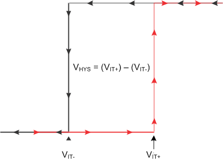
TLV4062 TLV4082 NonInvHyst.gifFigure 22. TLV40x2 Transfer Curve