ZHCSR71 October 2020 TLV4062-Q1 , TLV4082-Q1
PRODUCTION DATA
- 1 特性
- 2 应用
- 3 说明
- 4 Revision History
- 5 Pin Configuration and Functions
- 6 Specifications
- 7 Detailed Description
- 8 Application and Implementation
- 9 Power Supply Recommendations
- 10Layout
- 11Device and Documentation Support
5 Pin Configuration and Functions
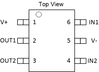
 Figure 5-1 DBV Package,
6-Pin SOT-23
Figure 5-1 DBV Package,
6-Pin SOT-23Table 5-1 Pin
Functions
| NAME | NO. | I/O | DESCRIPTION |
|---|---|---|---|
| DBV | |||
| GND | 5 | — | Ground |
| OUT1 | 2 | O | OUT1 is the output for
IN1. OUT1 is asserted (driven low) when the
voltage at IN1 falls below VIT–. OUT1
is deasserted (goes high) after IN1 rises higher
than VIT+. OUT1 is a push-pull output for the TLV4062 and an open-drain output for the TLV4082. The open-drain device (TLV4082) can be pulled up to 5.5 V independent of V+; a pullup resistor is required for this device. |
| OUT2 | 3 | O | OUT2 is the output for
IN2. OUT2 is asserted (driven low) when the
voltage at IN2 falls below VIT–. OUT2
is deasserted (goes high) after IN2 rises higher
than VIT+. OUT2 is a push-pull output for the TLV4062 and an open-drain output for the TLV4082. The open-drain device (TLV4082) can be pulled up to 5.5 V independent of V+; a pullup resistor is required for this device. |
| IN1 | 6 | I | This pin is connected
to the voltage to be monitored with the use of an
external resistor divider. When the voltage at this pin drops below the threshold voltage (VIT–), OUT1 is asserted. |
| IN2 | 4 | I | This pin is connected
to the voltage to be monitored with the use of an
external resistor divider. When the voltage at this pin drops below the threshold voltage (VIT–), OUT2 is asserted. |
| V+ | 1 | I | Supply voltage input. Connect a 1.5-V to 5.5-V supply to V+ in order to power the device. Good analog design practice is to place a 0.1-µF ceramic capacitor close to this pin (required for V+ < 1.5 V). |