ZHCSFX0B November 2016 – August 2017 TLV2316-Q1 , TLV316-Q1 , TLV4316-Q1
PRODUCTION DATA.
- 1 特性
- 2 应用
- 3 说明
- 4 修订历史记录
- 5 Device Comparison Table
- 6 Pin Configuration and Functions
- 7 Specifications
- 8 Detailed Description
- 9 Application and Implementation
- 10Power Supply Recommendations
- 11Layout
- 12器件和文档支持
- 13机械、封装和可订购信息
8 Detailed Description
8.1 Overview
The TLVx316-Q1 is a family of low-power, rail-to-rail input and output operational amplifiers. These devices operate from 1.8 V to 5.5 V, are unity-gain stable, and are suitable for a wide range of general-purpose applications. The class AB output stage is capable of driving ≤ 10-kΩ loads connected to any point between V+ and ground. The input common-mode voltage range includes both rails and allows the TLVx316-Q1 to be used in virtually any single-supply application. Rail-to-rail input and output swing significantly increases dynamic range, especially in low-supply applications, and makes them suitable for driving sampling analog-to-digital converters (ADCs).
The TLVx316-Q1 features 10-MHz bandwidth and 6-V/μs slew rate with only 400-μA supply current per channel, providing good ac performance at very-low-power consumption. DC applications are well served with a very-low input noise voltage of 12 nV/√Hz at 1 kHz, low input bias current (5 pA), and an input offset voltage of 0.5 mV (typical).
8.2 Functional Block Diagram

8.3 Feature Description
8.3.1 Operating Voltage
The TLVx316-Q1 operational amplifiers are fully specified and ensured for operation from 1.8 V to 5.5 V. In addition, many specifications apply from –40°C to +125°C. Parameters that vary significantly with operating voltages or temperature are illustrated in the Typical Characteristics section.
8.3.2 Rail-to-Rail Input
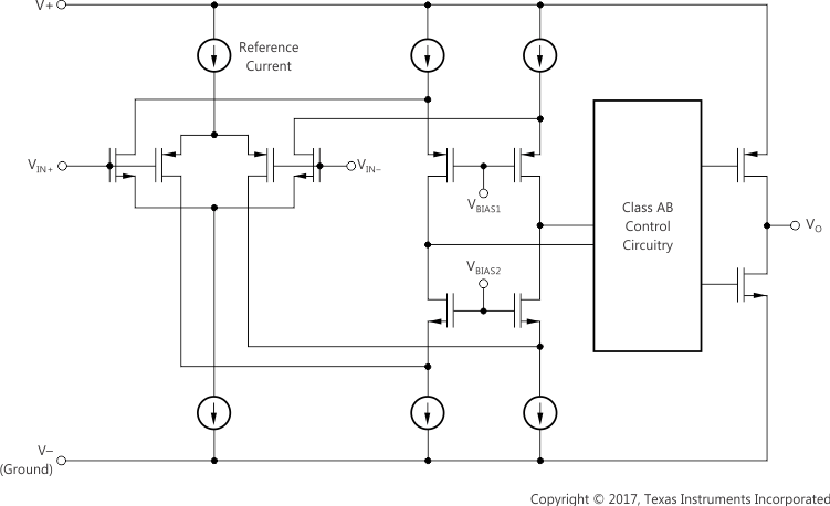
The input common-mode voltage range of the TLVx316-Q1 extends 200 mV beyond the supply rails for supply voltages greater than 2.5 V. This performance is achieved with a complementary input stage: an N-channel input differential pair in parallel with a P-channel differential pair, as shown in the Functional Block Diagram. The N-channel pair is active for input voltages close to the positive rail, typically (V+) – 1.4 V to 200 mV above the positive supply, whereas the P-channel pair is active for inputs from 200 mV below the negative supply to approximately (V+) – 1.4 V. There is a small transition region, typically (V+) – 1.2 V to (V+) – 1 V, in which both pairs are on. This 200-mV transition region can vary up to 200 mV with process variation. Thus, the transition region (both stages on) can range from (V+) – 1.4 V to (V+) – 1.2 V on the low end, up to (V+) – 1 V to (V+) – 0.8 V on the high end. Within this transition region, PSRR, CMRR, offset voltage, offset drift, and THD can be degraded compared to device operation outside this region.
8.3.3 Rail-to-Rail Output
Designed as a low-power, low-voltage operational amplifier, the TLVx316-Q1 delivers a robust output drive capability. A class AB output stage with common-source transistors is used to achieve full rail-to-rail output swing capability. For resistive loads of 10 kΩ, the output swings typically to within 30 mV of either supply rail regardless of the power-supply voltage applied. Different load conditions change the ability of the amplifier to swing close to the rails; see .
8.3.4 Common-Mode Rejection Ratio (CMRR)
CMRR for the TLVx316-Q1 is specified in two ways so the best match for a given application can be selected. The Electrical Characteristics table provides the CMRR of the device in the common-mode range below the transition region [VCM < (V+) – 1.4 V]. This specification is the best indicator of device capability when the application requires using one of the differential input pairs. The CMRR over the entire common-mode range is specified at VCM = –0.2 V to 5.7 V for VS = 5.5 V. This last value includes the variations through the transition region.
8.3.5 Capacitive Load and Stability
The TLVx316-Q1 is designed for applications where driving a capacitive load is required. As with all operational amplifiers, there may be specific instances where the TLVx316-Q1 can become unstable. The particular operational amplifier circuit configuration, layout, gain, and output loading are some of the factors to consider when establishing whether or not an amplifier is stable in operation. An operational amplifier in the unity-gain (1 V/V) buffer configuration that drives a capacitive load exhibits a greater tendency to be unstable than an amplifier operated at a higher noise gain. The capacitive load, in conjunction with the operational amplifier output resistance, creates a pole within the feedback loop that degrades the phase margin. The degradation of the phase margin increases when the capacitive loading increases. For a conservative best practice, designing for 25% overshoot (40° phase margin) provides improved stability over process variations. The equivalent series resistance (ESR) of some very-large capacitors (CL capacitors with a value greater than 1 μF) is sufficient to alter the phase characteristics in the feedback loop such that the amplifier remains stable. Increasing the amplifier closed-loop gain allows the amplifier to drive increasingly larger capacitance. This increased capability is evident when observing the overshoot response of the amplifier at higher voltage gains, as shown in Figure 7 (G = –1 V/V).
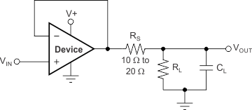
One technique for increasing the capacitive load drive capability of the amplifier operating in a unity-gain configuration is to insert a small resistor (typically 10-Ω to 20-Ω) in series with the output, as shown in Figure 14. This resistor significantly reduces the overshoot and ringing associated with large capacitive loads. One possible problem with this technique, however, is that a voltage divider is created with the added series resistor and any resistor connected in parallel with the capacitive load. The voltage divider introduces a gain error at the output that reduces the output swing.
 Figure 14. Improving Capacitive Load Drive
8.3.6 EMI Susceptibility and Input Filtering
Operational amplifiers vary with regard to the susceptibility of the device to electromagnetic interference (EMI). If conducted EMI enters the operational amplifier, the dc offset measured at the amplifier output can shift from the nominal value when EMI is present. This shift is a result of signal rectification associated with the internal semiconductor junctions. Although EMI can affect all operational amplifier pin functions, the signal input pins are likely to be the most susceptible. The TLVx316-Q1 operational amplifier family incorporates an internal input low-pass filter that reduces the amplifier response to EMI. This filter provides both common-mode and differential-mode filtering. The filter is designed for a cutoff frequency of approximately 80 MHz (–3 dB), with a roll-off of 20 dB per decade.
The immunity of an operational amplifier can be accurately measured and quantified over a broad frequency spectrum extending from 10 MHz to 6 GHz. The EMI rejection ratio (EMIRR) metric allows operational amplifiers to be directly compared by the EMI immunity. Figure 12 illustrates the results of this testing on the TLVx316-Q1. Detailed information can be found in EMI Rejection Ratio of Operational Amplifiers, available for download from www.ti.com.
8.3.7 Overload Recovery
Overload recovery is defined as the time required for the operational amplifier output to recover from a saturated state to a linear state. The output devices of the operational amplifier enter a saturation region when the output voltage exceeds the rated operating voltage, either because of the high input voltage or the high gain. After the device enters the saturation region, the charge carriers in the output devices require time to return back to the linear state. After the charge carriers return back to the linear state, the device begins to slew at the specified slew rate. Thus, the propagation delay in case of an overload condition is the sum of the overload recovery time and the slew time. The overload recovery time for the TLVx316-Q1 is approximately 300 ns.
8.4 Device Functional Modes
The TLVx316-Q1 family has a single functional mode. These devices are powered on as long as the power-supply voltage is between 1.8 V (±0.9 V) and 5.5 V (±2.75 V).