SNOSDF0 May   2024 TLV4H290-SEP , TLV4H390-SEP

ADVANCE INFORMATION  

  1.   1
  2. Features
  3. Applications
  4. Description
  5. Pin Configuration and Functions
    1. 4.1 Pin Functions:TLV4H290-SEP and TLV4H390-SEP Quad
  6. Specifications
    1. 5.1 Absolute Maximum Ratings
    2. 5.2 ESD Ratings
    3. 5.3 Recommended Operating Conditions
    4. 5.4 Thermal Information, Quad
    5. 5.5 Electrical Characteristics, Quad
    6. 5.6 Switching Characteristics, Quad
    7. 5.7 Typical Characteristics
  7. Detailed Description
    1. 6.1 Overview
    2. 6.2 Functional Block Diagram
    3. 6.3 Feature Description
    4. 6.4 Device Functional Modes
      1. 6.4.1 Outputs
        1. 6.4.1.1 TLV4H290-SEP Open Drain Output
        2. 6.4.1.2 TLV4H390-SEP Push-Pull Output
      2. 6.4.2 Power-On Reset (POR)
      3. 6.4.3 Inputs
        1. 6.4.3.1 Rail to Rail Input
        2. 6.4.3.2 Fault Tolerant Inputs
        3. 6.4.3.3 Input Protection
      4. 6.4.4 ESD Protection
      5. 6.4.5 Unused Inputs
      6. 6.4.6 Hysteresis
  8. Application and Implementation
    1. 7.1 Application Information
      1. 7.1.1 Basic Comparator Definitions
        1. 7.1.1.1 Operation
        2. 7.1.1.2 Propagation Delay
        3. 7.1.1.3 Overdrive Voltage
      2. 7.1.2 Hysteresis
        1. 7.1.2.1 Inverting Comparator With Hysteresis
        2. 7.1.2.2 Non-Inverting Comparator With Hysteresis
        3. 7.1.2.3 Inverting and Non-Inverting Hysteresis using Open-Drain Output
    2. 7.2 Typical Applications
      1. 7.2.1 Window Comparator
        1. 7.2.1.1 Design Requirements
        2. 7.2.1.2 Detailed Design Procedure
        3. 7.2.1.3 Application Curve
      2. 7.2.2 Square-Wave Oscillator
        1. 7.2.2.1 Design Requirements
        2. 7.2.2.2 Detailed Design Procedure
        3. 7.2.2.3 Application Curve
      3. 7.2.3 Adjustable Pulse Width Generator
      4. 7.2.4 Time Delay Generator
      5. 7.2.5 Logic Level Shifter
      6. 7.2.6 One-Shot Multivibrator
      7. 7.2.7 Bi-Stable Multivibrator
      8. 7.2.8 Zero Crossing Detector
      9. 7.2.9 Pulse Slicer
    3. 7.3 Power Supply Recommendations
    4. 7.4 Layout
      1. 7.4.1 Layout Guidelines
      2. 7.4.2 Layout Example
  9. Device and Documentation Support
    1. 8.1 Documentation Support
      1. 8.1.1 Related Documentation
    2. 8.2 Receiving Notification of Documentation Updates
    3. 8.3 Support Resources
    4. 8.4 Trademarks
    5. 8.5 Electrostatic Discharge Caution
    6. 8.6 Glossary
  10. Revision History
  11. 10Mechanical, Packaging, and Orderable Information

封装选项

机械数据 (封装 | 引脚)
散热焊盘机械数据 (封装 | 引脚)
订购信息

Time Delay Generator

The circuit shown in Figure 7-13 provides output signals at a prescribed time interval from a time reference and automatically resets the output low when the input returns to 0V. This is useful for sequencing a "power on" signal to trigger a controlled start-up of power supplies.
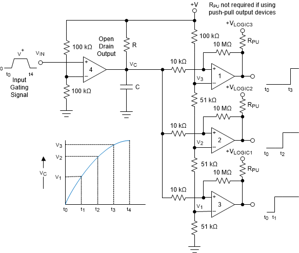
TLV4H290-SEP TLV4H390-SEP Time Delay GeneratorFigure 7-13 Time Delay Generator

Consider the case of VIN = 0. The output of comparator 4 is also at ground, "shorting" the capacitor and holding it at 0V. This implies that the outputs of comparators 1, 2, and 3 are also at 0V. When an input signal is applied, the output of open drain comparator 4 goes High-Z and C charges exponentially through R. This is indicated in the graph. The output voltages of comparators 1, 2, and 3 switch to the high state in sequence when VC rises above the reference voltages V1, V2 and V3. A small amount of hysteresis has been provided by the 10kΩ and 10MΩ resistors to insure fast switching when the RC time constant is chosen to give long delay times. A good starting point is R = 100kΩ and C = 0.01µF to 1µF.

All outputs immediately go low when VIN falls to 0V, due to the comparator output going low and immediately discharging the capacitor.

Comparator 4 must be a open-drain type output (TLV4H290-SEP), whereas comparators 1 though 3 may be either open drain or push-pull output, depending on system requirements. RPU is not required for push-pull output devices.