SNOSDF0 May   2024 TLV4H290-SEP , TLV4H390-SEP

ADVANCE INFORMATION  

  1.   1
  2. Features
  3. Applications
  4. Description
  5. Pin Configuration and Functions
    1. 4.1 Pin Functions:TLV4H290-SEP and TLV4H390-SEP Quad
  6. Specifications
    1. 5.1 Absolute Maximum Ratings
    2. 5.2 ESD Ratings
    3. 5.3 Recommended Operating Conditions
    4. 5.4 Thermal Information, Quad
    5. 5.5 Electrical Characteristics, Quad
    6. 5.6 Switching Characteristics, Quad
    7. 5.7 Typical Characteristics
  7. Detailed Description
    1. 6.1 Overview
    2. 6.2 Functional Block Diagram
    3. 6.3 Feature Description
    4. 6.4 Device Functional Modes
      1. 6.4.1 Outputs
        1. 6.4.1.1 TLV4H290-SEP Open Drain Output
        2. 6.4.1.2 TLV4H390-SEP Push-Pull Output
      2. 6.4.2 Power-On Reset (POR)
      3. 6.4.3 Inputs
        1. 6.4.3.1 Rail to Rail Input
        2. 6.4.3.2 Fault Tolerant Inputs
        3. 6.4.3.3 Input Protection
      4. 6.4.4 ESD Protection
      5. 6.4.5 Unused Inputs
      6. 6.4.6 Hysteresis
  8. Application and Implementation
    1. 7.1 Application Information
      1. 7.1.1 Basic Comparator Definitions
        1. 7.1.1.1 Operation
        2. 7.1.1.2 Propagation Delay
        3. 7.1.1.3 Overdrive Voltage
      2. 7.1.2 Hysteresis
        1. 7.1.2.1 Inverting Comparator With Hysteresis
        2. 7.1.2.2 Non-Inverting Comparator With Hysteresis
        3. 7.1.2.3 Inverting and Non-Inverting Hysteresis using Open-Drain Output
    2. 7.2 Typical Applications
      1. 7.2.1 Window Comparator
        1. 7.2.1.1 Design Requirements
        2. 7.2.1.2 Detailed Design Procedure
        3. 7.2.1.3 Application Curve
      2. 7.2.2 Square-Wave Oscillator
        1. 7.2.2.1 Design Requirements
        2. 7.2.2.2 Detailed Design Procedure
        3. 7.2.2.3 Application Curve
      3. 7.2.3 Adjustable Pulse Width Generator
      4. 7.2.4 Time Delay Generator
      5. 7.2.5 Logic Level Shifter
      6. 7.2.6 One-Shot Multivibrator
      7. 7.2.7 Bi-Stable Multivibrator
      8. 7.2.8 Zero Crossing Detector
      9. 7.2.9 Pulse Slicer
    3. 7.3 Power Supply Recommendations
    4. 7.4 Layout
      1. 7.4.1 Layout Guidelines
      2. 7.4.2 Layout Example
  9. Device and Documentation Support
    1. 8.1 Documentation Support
      1. 8.1.1 Related Documentation
    2. 8.2 Receiving Notification of Documentation Updates
    3. 8.3 Support Resources
    4. 8.4 Trademarks
    5. 8.5 Electrostatic Discharge Caution
    6. 8.6 Glossary
  10. Revision History
  11. 10Mechanical, Packaging, and Orderable Information

封装选项

机械数据 (封装 | 引脚)
散热焊盘机械数据 (封装 | 引脚)
订购信息

Adjustable Pulse Width Generator

Figure 7-12 is a variation on the square wave oscillator that allows adjusting the pulse widths.

R4 and R5 provide separate charge and discharge paths for the capacitor C depending on the output state.
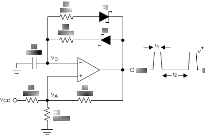
TLV4H290-SEP TLV4H390-SEP Adjustable Pulse Width GeneratorFigure 7-12 Adjustable Pulse Width Generator

The charge path is set through R5 and D2 when the output is high. Similarly, the discharge path for the capacitor is set by R4 and D1 when the output is low.

The pulse width t1 is determined by the RC time constant of R5 and C. Thus, the time t2 between the pulses can be changed by varying R4, and the pulse width can be altered by R5. The frequency of the output can be changed by varying both R4 and R5. At low voltages, the effects of the diode forward drop (0.8V, or 0.15V for Shottky) must be taken into account by altering output high and low voltages in the calculations.