ZHCSIO7A August   2018  – December 2018 TLV6001-Q1 , TLV6002-Q1

PRODUCTION DATA.  

  1. 特性
  2. 应用
  3. 说明
    1.     CMRR 和 PSRR 与温度间的关系
  4. 修订历史记录
  5. Pin Configuration and Functions
    1.     Pin Functions: TLV6001-Q1
    2.     Pin Functions: TLV6002-Q1
  6. Specifications
    1. 6.1 Absolute Maximum Ratings
    2. 6.2 ESD Ratings
    3. 6.3 Recommended Operating Conditions
    4. 6.4 Thermal Information: TLV6001-Q1
    5. 6.5 Thermal Information: TLV6002-Q1
    6. 6.6 Electrical Characteristics: VS = 1.8 V to 5 V (±0.9 V to ±2.75 V)
    7. 6.7 Typical Characteristics: Table of Graphs
    8. 6.8 Typical Characteristics
  7. Detailed Description
    1. 7.1 Overview
    2. 7.2 Functional Block Diagram
    3. 7.3 Feature Description
      1. 7.3.1 Operating Voltage
      2. 7.3.2 Rail-to-Rail Input
      3. 7.3.3 Rail-to-Rail Output
      4. 7.3.4 Common-Mode Rejection Ratio (CMRR)
      5. 7.3.5 Capacitive Load and Stability
      6. 7.3.6 EMI Susceptibility and Input Filtering
    4. 7.4 Device Functional Modes
    5. 7.5 Input and ESD Protection
  8. Application and Implementation
    1. 8.1 Application Information
    2. 8.2 Typical Application
      1. 8.2.1 Design Requirements
      2. 8.2.2 Detailed Design Procedure
      3. 8.2.3 Application Curve
    3. 8.3 System Examples
  9. Power Supply Recommendations
  10. 10Layout
    1. 10.1 Layout Guidelines
    2. 10.2 Layout Example: Single Channel
    3. 10.3 Layout Example: Dual Channel
  11. 11器件和文档支持
    1. 11.1 文档支持
      1. 11.1.1 相关文档
    2. 11.2 相关链接
    3. 11.3 接收文档更新通知
    4. 11.4 社区资源
    5. 11.5 商标
    6. 11.6 静电放电警告
    7. 11.7 术语表
  12. 12机械、封装和可订购信息

封装选项

请参考 PDF 数据表获取器件具体的封装图。

机械数据 (封装 | 引脚)
  • DCK|5
散热焊盘机械数据 (封装 | 引脚)
订购信息

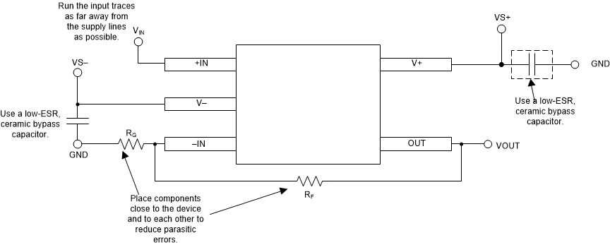
Layout Example: Single Channel

TLV6001-Q1 TLV6002-Q1 SC70_layout_example_SBOS779.gifFigure 25. Operational Amplifier Board Layout for Noninverting Configuration
TLV6001-Q1 TLV6002-Q1 sch_rep_sbos785.gifFigure 26. Schematic Representation of Figure 25