ZHCSIO7A August 2018 – December 2018 TLV6001-Q1 , TLV6002-Q1
PRODUCTION DATA.
- 1 特性
- 2 应用
- 3 说明
- 4 修订历史记录
- 5 Pin Configuration and Functions
- 6 Specifications
- 7 Detailed Description
- 8 Application and Implementation
- 9 Power Supply Recommendations
- 10Layout
- 11器件和文档支持
- 12机械、封装和可订购信息
封装选项
请参考 PDF 数据表获取器件具体的封装图。
机械数据 (封装 | 引脚)
- D|8
- DGK|8
散热焊盘机械数据 (封装 | 引脚)
订购信息
7.3.5 Capacitive Load and Stability
The TLV600x-Q1 family is designed to be used in applications where driving a capacitive load is required. As with all operational amplifiers, there can be specific instances where the TLV600x-Q1 family can become unstable. The particular op amp circuit configuration, layout, gain, and output loading are some of the factors to consider when establishing if an amplifier is stable in operation. An operational amplifier in the unity-gain (1-V/V) buffer configuration that drives a capacitive load exhibits a greater tendency for instability than an amplifier that is operated at a higher noise gain. The capacitive load in conjunction with the op amp output resistance creates a pole within the feedback loop that degrades the phase margin. The degradation of the phase margin increases as the capacitive loading increases. When operating in the unity-gain configuration, the TLV600x-Q1 family remains stable with a pure capacitive load up to approximately 1 nF. The equivalent series resistance (ESR) of some capacitors (CL greater than 1 µF) is sufficient to alter the phase characteristics in the feedback loop such that the amplifier remains stable. Increasing the amplifier closed-loop gain allows the amplifier to drive increasingly larger capacitance. This increased capability is evident when observing the overshoot response of the amplifier at higher voltage gains.
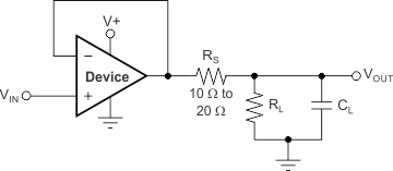
One technique for increasing the capacitive load drive capability of the amplifier when the device operates in a unity-gain configuration is to insert a small resistor, typically 10 Ω to 20 Ω, in series with the output, as Figure 19 shows. This resistor reduces the overshoot and ringing associated with large capacitive loads. One possible problem with this technique is that a voltage divider is created with the added series resistor and any resistor connected in parallel with the capacitive load. The voltage divider introduces a gain error at the output that reduces the output swing.
 Figure 19. Improving Capacitive Load Drive