SLVSAC4B November 2010 – December 2015 TLV62065
PRODUCTION DATA.
- 1 Features
- 2 Applications
- 3 Description
- 4 Revision History
- 5 Pin Configuration and Functions
- 6 Specifications
- 7 Detailed Description
- 8 Application and Implementation
- 9 Power Supply Recommendations
- 10Layout
- 11Device and Documentation Support
- 12Mechanical, Packaging, and Orderable Information
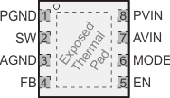
5 Pin Configuration and Functions
DSG Package
8-Pin WSON
Top View

Pin Functions
| PIN | TYPE(1) | DESCRIPTION | ||
|---|---|---|---|---|
| NAME | NO. | |||
| AGND | 3 | I | Analog GND supply pin for the control circuit. | |
| AVIN | 7 | I | Analog VIN power supply for the control circuit. Need to be connected to PVIN and input capacitor. | |
| EN | 5 | I | This is the enable pin of the device. Pulling this pin to low forces the device into shutdown mode. Pulling this pin to high enables the device. This pin must be terminated | |
| Exposed Thermal Pad | — | — | For good thermal performance, this pad must be soldered to the land pattern on the PCB. This pad should be used as device GND. | |
| FB | 4 | I | Feedback pin for the internal regulation loop. Connect the external resistor divider to this pin. In case of fixed output voltage option, connect this pin directly to the output capacitor | |
| MODE | 6 | I | MODE pin = High forces the device to operate in fixed frequency PWM mode. MODE pin = Low enables the power save mode with automatic transition from PFM mode to fixed frequency PWM mode. This pin must be terminated. | |
| PGND | 1 | P | GND supply pin for the output stage. | |
| PVIN | 8 | P | VIN power supply pin for the output stage. | |
| SW | 2 | O | This is the switch pin and is connected to the internal MOSFET switches. Connect the external inductor between this terminal and the output capacitor. | |
(1) I = Input, O = Output, P = Power