ZHCSDM0B October 2013 – December 2014 TLV62565 , TLV62566
PRODUCTION DATA.
- 1 特性
- 2 应用
- 3 说明
- 4 简化电路原理图
- 5 修订历史记录
- 6 Device Comparison Table
- 7 Pin Configuration and Functions
- 8 Specifications
- 9 Parameter Measurement Information
- 10Detailed Description
- 11Application and Implementation
- 12Power Supply Recommendations
- 13Layout
- 14器件和文档支持
- 15机械、封装和可订购信息
13 Layout
13.1 Layout Guidelines
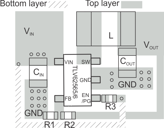
The PCB layout is an important step to maintain the high performance of the TLV62565 devices.
- The input/output capacitors and the inductor should be placed as close as possible to the IC.
- This keeps the traces short. Routing these traces direct and wide results in low trace resistance and low parasitic inductance.
- A common power GND should be used.
- The low side of the input and output capacitors must be connected properly to the power GND to avoid a GND potential shift.
- The sense traces connected to FB is a signal trace .
- Special care should be taken to avoid noise being induced. By a direct routing, parasitic inductance can be kept small.
- GND layers might be used for shielding.
- Keep these traces away from SW nodes .
13.2 Layout Example

13.3 Thermal Considerations
Implementation of integrated circuits in low-profile and fine-pitch surface-mount packages typically requires special attention to power dissipation. Many system-dependent issues such as thermal coupling, airflow, convection surfaces, and the presence of other heat-generating components affect the power dissipation limits of a given component.
Two basic approaches for enhancing thermal performance are listed below:
- Improving the power dissipation capability of the PCB design
- Introducing airflow in the system
For more details on how to use the thermal parameters, see the application notes: Thermal Characteristics Application Notes SZZA017 and SPRA953.