ZHCSDM0B October 2013 – December 2014 TLV62565 , TLV62566
PRODUCTION DATA.
- 1 特性
- 2 应用
- 3 说明
- 4 简化电路原理图
- 5 修订历史记录
- 6 Device Comparison Table
- 7 Pin Configuration and Functions
- 8 Specifications
- 9 Parameter Measurement Information
- 10Detailed Description
- 11Application and Implementation
- 12Power Supply Recommendations
- 13Layout
- 14器件和文档支持
- 15机械、封装和可订购信息
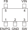
7 Pin Configuration and Functions
5-Pin SOT-23
DBV Package
(Top View)

Pin Functions
| PIN | I/O/PWR | DESCRIPTION | ||
|---|---|---|---|---|
| NAME | NUMBER | |||
| TLV62565 | TLV62566 | |||
| EN | 1 | — | I | Device enable logic input. Logic HIGH enables the device, logic low disables the device and turns it into shutdown. |
| FB | 5 | 5 | I | Feedback pin for the internal control loop. Connect this pin to the external feedback divider. |
| GND | 2 | 2 | PWR | Ground pin. |
| PG | — | 1 | O | Power Good open drain output. This pin is high impedance if the output voltage is within regulation. It is pulled low if the output is below its nominal value. It is also in logic low when VIN below UVLO or thermal shutdown triggers. |
| SW | 3 | 3 | PWR | Switch pin connected to the internal MOSFET switches and inductor terminal. Connect the inductor of the output filter to this pin. |
| VIN | 4 | 4 | PWR | Power supply voltage input. |