ZHCSFQ3B November 2016 – November 2017 TLV62568
PRODUCTION DATA.
- 1 特性
- 2 应用
- 3 说明
- 4 修订历史记录
- 5 Pin Configuration and Functions
- 6 Specifications
- 7 Detailed Description
- 8 Application and Implementation
- 9 Power Supply Recommendations
- 10Layout
- 11器件和文档支持
- 12机械、封装和可订购信息
封装选项
机械数据 (封装 | 引脚)
散热焊盘机械数据 (封装 | 引脚)
订购信息
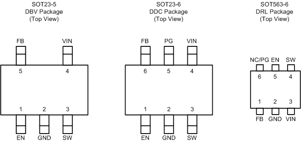
5 Pin Configuration and Functions

Pin Functions
| PIN NUMBER | I/O/PWR | DESCRIPTION | |||
|---|---|---|---|---|---|
| NAME | SOT23-5 | SOT23-6 | SOT563-6 | ||
| EN | 1 | 1 | 5 | I | Device enable logic input. Logic high enables the device, logic low disables the device and turns it into shutdown. Do not leave floating. |
| GND | 2 | 2 | 2 | PWR | Ground pin. |
| SW | 3 | 3 | 4 | PWR | Switch pin connected to the internal FET switches and inductor terminal. Connect the inductor of the output filter to this pin. |
| VIN | 4 | 4 | 3 | PWR | Power supply voltage input. |
| PG | - | 5 | 6 | O | Power good open drain output pin for TLV62568P. The pull-up resistor should not be connected to any voltage higher than 5.5V. If it's not used, leave the pin floating. |
| FB | 5 | 6 | 1 | I | Feedback pin for the internal control loop. Connect this pin to an external feedback divider. |
| NC | - | - | 6 | O | No connection pin for TLV62568DRL. The pin can be connected to the output. Or leave it floating. |