ZHCSFQ3B November 2016 – November 2017 TLV62568
PRODUCTION DATA.
- 1 特性
- 2 应用
- 3 说明
- 4 修订历史记录
- 5 Pin Configuration and Functions
- 6 Specifications
- 7 Detailed Description
- 8 Application and Implementation
- 9 Power Supply Recommendations
- 10Layout
- 11器件和文档支持
- 12机械、封装和可订购信息
封装选项
机械数据 (封装 | 引脚)
散热焊盘机械数据 (封装 | 引脚)
订购信息
7 Detailed Description
7.1 Overview
The TLV62568 is a high-efficiency synchronous step-down converter. The device operates with an adaptive off-time with peak current control scheme. The device operates at typically 1.5-MHz frequency pulse width modulation (PWM) at moderate to heavy load currents. Based on the VIN/VOUT ratio, a simple circuit sets the required off time for the low-side MOSFET. It makes the switching frequency relatively constant regardless of the variation of input voltage, output voltage, and load current.
7.2 Functional Block Diagram
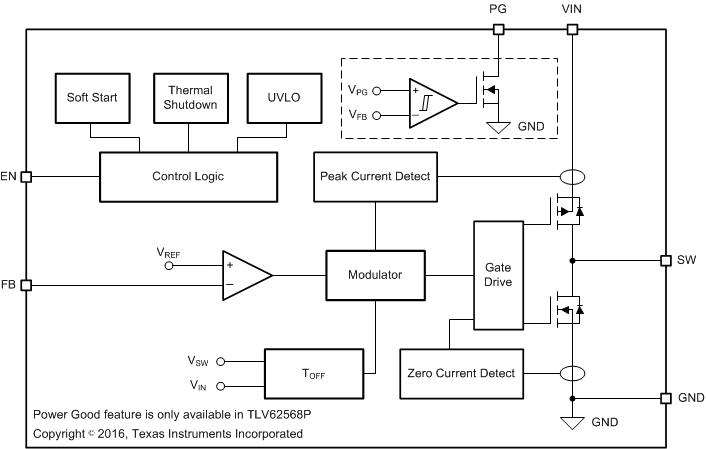
 Figure 4. TLV62568 Functional Block Diagram
7.3 Feature Description
7.3.1 Power Save Mode
The device automatically enters Power Save Mode to improve efficiency at light load when the inductor current becomes discontinuous. In Power Save Mode, the converter reduces switching frequency and minimizes current consumption. In Power Save Mode, the output voltage rises slightly above the nominal output voltage. This effect is minimized by increasing the output capacitor.
7.3.2 100% Duty Cycle Low Dropout Operation
The device offers a low input-to-output voltage differential by entering 100% duty cycle mode. In this mode, the high-side MOSFET switch is constantly turned on and the low-side MOSFET is switched off. The minimum input voltage to maintain output regulation, depending on the load current and output voltage, is calculated as:
where
- RDS(ON) = High side FET on-resistance
- RL = Inductor ohmic resistance (DCR)
7.3.3 Soft Startup
After enabling the device, internal soft startup circuitry ramps up the output voltage which reaches nominal output voltage during a startup time. This avoids excessive inrush current and creates a smooth output voltage rise slope. It also prevents excessive voltage drops of primary cells and rechargeable batteries with high internal impedance.
The TLV62568 is able to start into a pre-biased output capacitor. The converter starts with the applied bias voltage and ramps the output voltage to its nominal value.
7.3.4 Switch Current Limit
The switch current limit prevents the device from high inductor current and drawing excessive current from a battery or input voltage rail. Excessive current might occur with a heavy load or shorted output circuit condition. The TLV62568 adopts the peak current control by sensing the current of the high-side switch. Once the high-side switch current limit is reached, the high-side switch is turned off and low-side switch is turned on to ramp down the inductor current with an adaptive off-time.
7.3.5 Under Voltage Lockout
To avoid mis-operation of the device at low input voltages, under voltage lockout is implemented that shuts down the device at voltages lower than VUVLO with VHYS_UVLO hysteresis.
7.3.6 Thermal Shutdown
The device enters thermal shutdown once the junction temperature exceeds the thermal shutdown rising threshold, TJSD. Once the junction temperature falls below the falling threshold, the device returns to normal operation automatically.
7.4 Device Functional Modes
7.4.1 Enabling/Disabling the Device
The device is enabled by setting the EN input to a logic High. Accordingly, a logic Low disables the device. If the device is enabled, the internal power stage starts switching and regulates the output voltage to the set point voltage. The EN input must be terminated and should not be left floating.
7.4.2 Power Good
The TLV62568P has a power good output. The PG pin goes high impedance once the output is above 95% of the nominal voltage, and is driven low once the output voltage falls below typically 90% of the nominal voltage. The PG pin is an open-drain output and is specified to sink up to 1 mA. The power good output requires a pull-up resistor connecting to any voltage rail less than 5.5 V. The PG signal can be used for sequencing of multiple rails by connecting it to the EN pin of other converters. Leave the PG pin unconnected when not used.
Table 1. PG Pin Logic
| DEVICE CONDITIONS | LOGIC STATUS | ||
|---|---|---|---|
| HIGH Z | LOW | ||
| Enable | EN = High, VFB ≥ VPG | √ | |
| EN = High, VFB ≤ VPG | √ | ||
| Shutdown | EN = Low | √ | |
| Thermal Shutdown | TJ > TJSD | √ | |
| UVLO | 1.4 V < VIN < VUVLO | √ | |
| Power Supply Removal | VIN ≤ 1.4 V | √ | |