ZHCSGK2F November   2019  – November 2019 TLV62585

PRODUCTION DATA.  

  1. 特性
  2. 应用
  3. 说明
    1.     Device Images
      1.      典型应用原理图
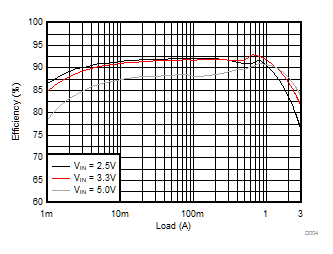
      2.      5V 输入电压效率
  4. 修订历史记录
  5. Pin Configuration and Functions
    1.     Pin Functions
  6. Specifications
    1. 6.1 Absolute Maximum Ratings
    2. 6.2 ESD Ratings
    3. 6.3 Recommended Operating Conditions
    4. 6.4 Thermal Information
    5. 6.5 Electrical Characteristics
    6. 6.6 Typical Characteristics
  7. Detailed Description
    1. 7.1 Overview
    2. 7.2 Functional Block Diagram
    3. 7.3 Feature Description
      1. 7.3.1 Power Save Mode
      2. 7.3.2 100% Duty Cycle Low Dropout Operation
      3. 7.3.3 Soft Start
      4. 7.3.4 Switch Current Limit and Short Circuit Protection (HICCUP)
      5. 7.3.5 Undervoltage Lockout
      6. 7.3.6 Thermal Shutdown
    4. 7.4 Device Functional Modes
      1. 7.4.1 Enable and Disable
      2. 7.4.2 Power Good
  8. Application and Implementation
    1. 8.1 Application Information
    2. 8.2 Typical Application
      1. 8.2.1 Design Requirements
      2. 8.2.2 Detailed Design Procedure
        1. 8.2.2.1 Custom Design With WEBENCH® Tools
        2. 8.2.2.2 Setting The Output Voltage
        3. 8.2.2.3 Output Filter Design
        4. 8.2.2.4 Inductor Selection
        5. 8.2.2.5 Input and Output Capacitor Selection
      3. 8.2.3 Application Curves
  9. Power Supply Recommendations
  10. 10Layout
    1. 10.1 Layout Guidelines
    2. 10.2 Layout Example
    3. 10.3 Thermal Considerations
  11. 11器件和文档支持
    1. 11.1 器件支持
      1. 11.1.1 第三方米6体育平台手机版_好二三四免责声明
      2. 11.1.2 使用 WEBENCH® 工具创建定制设计方案
    2. 11.2 文档支持
      1. 11.2.1 相关文档
    3. 11.3 接收文档更新通知
    4. 11.4 支持资源
    5. 11.5 商标
    6. 11.6 静电放电警告
    7. 11.7 Glossary
  12. 12机械、封装和可订购信息

封装选项

机械数据 (封装 | 引脚)
散热焊盘机械数据 (封装 | 引脚)
订购信息

Application Curves

VIN = 5 V, VOUT = 1.8 V, TA = 25 ºC, unless otherwise noted.
TLV62585 D004_SLVSDE5_TLV62585.gif
VOUT = 1.2 V
Figure 5. Efficiency
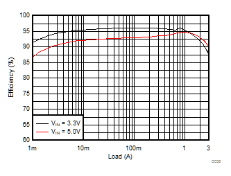
TLV62585 D006_SLVSDE5_TLV62585.gif
VOUT = 2.5 V
Figure 7. Efficiency
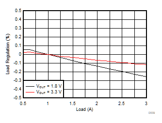
TLV62585 D009_SLVSDE5_TLV62585.gif
VIN = 5 V
Figure 9. Load Regulation
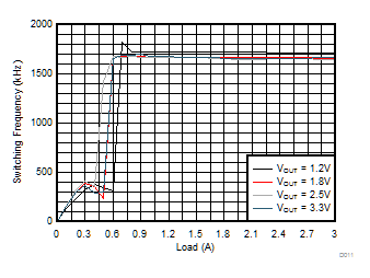
TLV62585 D011_SLVSDE5_TLV62585.gif
VIN = 5 V
Figure 11. Switching Frequency
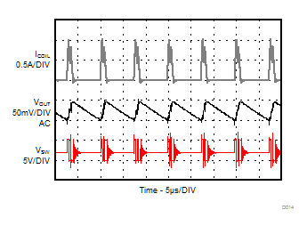
TLV62585 D014_SLVSDE5_TLV62585.gif
IOUT = 0.1 A
Figure 13. PSM Operation
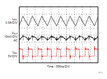
TLV62585 D013_SLVSDE5_TLV62585.gif
IOUT = 3 A
Figure 15. PWM Operation
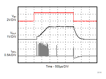
TLV62585 D016_SLVSDE5_TLV62585.gif
No Load
Figure 17. Start-Up and Shut-Down without Load
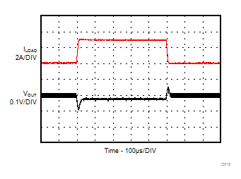
TLV62585 D018_SLVSDE5_TLV62585.gif
IOUT = 0.1 A to 3 A C3 = 22 pF
Figure 19. Load Transient with A Feedforward Capacitor
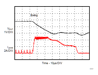
TLV62585 D021_SLVSDE5_TLV62585.gif
IOUT = 0.1 A
Figure 21. Output Short Protection (HICCUP) - Zoom In
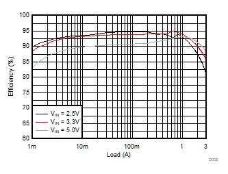
TLV62585 D005_SLVSDE5_TLV62585.gif
VOUT = 1.8 V
Figure 6. Efficiency
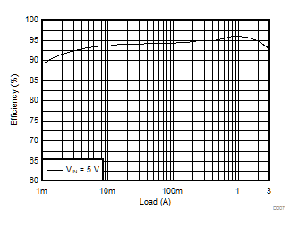
TLV62585 D007_SLVSDE5_TLV62585.gif
VOUT = 3.3 V
Figure 8. Efficiency
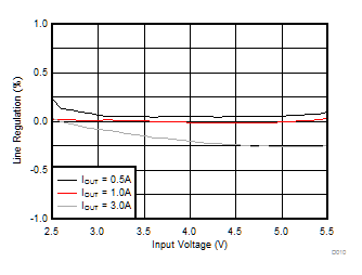
TLV62585 D010_SLVSDE5_TLV62585.gif
VOUT = 1.8 V
Figure 10. Line Regulation
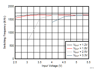
TLV62585 D012_SLVSDE5_TLV62585.gif
IOUT = 1 A
Figure 12. Switching Frequency
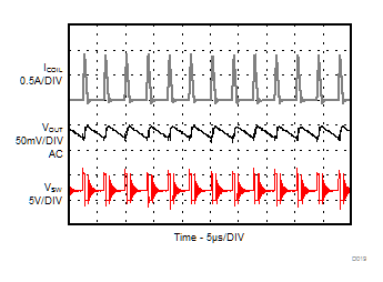
TLV62585 D019_SLVSDE5_TLV62585.gif
IOUT = 0.1 A C3 = 22 pF
Figure 14. PSM Operation with A Feedforward Capacitor
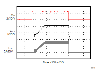
TLV62585 D015_SLVSDE5_TLV62585.gif
ROUT = 0.6 Ω
Figure 16. Start-Up and Shut-Down with Load
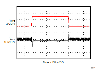
TLV62585 D017_SLVSDE5_TLV62585.gif
IOUT = 0.1 A to 3 A
Figure 18. Load Transient
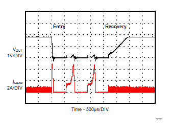
TLV62585 D020_SLVSDE5_TLV62585.gif
IOUT = 0.1 A
Figure 20. Output Short Protection (HICCUP)
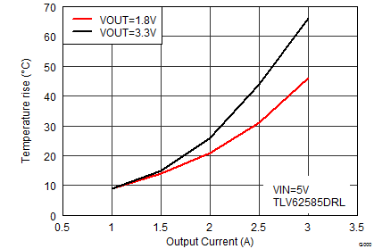
TLV62585 SLVSDE5_temprise_DRL.gif
Figure 22. Temperature Rise of DRL Package on EVM