ZHCSHH1B January   2018  – November 2019 TLV6700

PRODUCTION DATA.  

  1. 特性
  2. 应用
  3. 说明
    1.     Device Images
      1.      简化方框图
      2.      输出响应
  4. 修订历史记录
  5. Device Comparison Table
  6. Pin Configuration and Functions
    1.     Pin Functions
  7. Specifications
    1. 7.1 Absolute Maximum Ratings
    2. 7.2 ESD Ratings
    3. 7.3 Recommended Operating Conditions
    4. 7.4 Thermal Information
    5. 7.5 Electrical Characteristics
    6. 7.6 Timing Requirements
    7. 7.7 Switching Characteristics
    8. 7.8 Typical Characteristics
  8. Detailed Description
    1. 8.1 Overview
    2. 8.2 Functional Block Diagram
    3. 8.3 Feature Description
      1. 8.3.1 Inputs (INA+, INB–)
      2. 8.3.2 Outputs (OUTA, OUTB)
      3. 8.3.3 Window Comparator
      4. 8.3.4 Immunity to Input Terminal Voltage Transients
    4. 8.4 Device Functional Modes
      1. 8.4.1 Normal Operation (VDD > UVLO)
      2. 8.4.2 Undervoltage Lockout (V(POR) < VDD < UVLO)
      3. 8.4.3 Power-On Reset (VDD < V(POR))
  9. Application and Implementation
    1. 9.1 Application Information
      1. 9.1.1 VPULLUP to a Voltage Other Than VDD
      2. 9.1.2 Monitoring VDD
      3. 9.1.3 Monitoring a Voltage Other Than VDD
    2. 9.2 Typical Application
      1. 9.2.1 Design Requirements
      2. 9.2.2 Detailed Design Procedure
        1. 9.2.2.1 Resistor Divider Selection
        2. 9.2.2.2 Pullup Resistor Selection
        3. 9.2.2.3 Input Supply Capacitor
        4. 9.2.2.4 Input Capacitors
      3. 9.2.3 Application Curves
    3. 9.3 Do's and Don'ts
  10. 10Power Supply Recommendations
  11. 11Layout
    1. 11.1 Layout Guidelines
    2. 11.2 Layout Example
  12. 12器件和文档支持
    1. 12.1 器件支持
      1. 12.1.1 开发支持
    2. 12.2 接收文档更新通知
    3. 12.3 社区资源
    4. 12.4 商标
    5. 12.5 静电放电警告
    6. 12.6 Glossary
  13. 13机械、封装和可订购信息

封装选项

机械数据 (封装 | 引脚)
散热焊盘机械数据 (封装 | 引脚)
订购信息

Typical Characteristics

at TJ = 25°C and VDD = 5 V (unless otherwise noted)
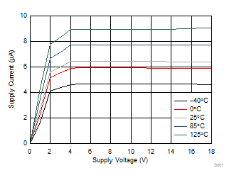
TLV6700 D002_SLVSCI7.gif
Figure 2. Supply Current (IDD) vs Supply Voltage (VDD)
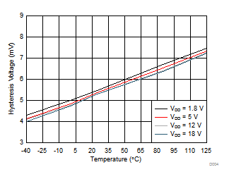
TLV6700 D004_SLVSCI7.gif
Figure 4. Hysteresis (Vhys) vs Temperature
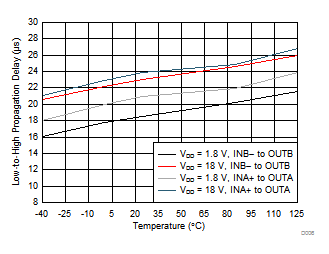
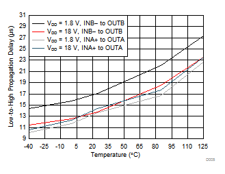
TLV6700 D006_SLVSCI7.gif
Figure 6. Propagation Delay vs Temperature
(Low-to-High Transition at the Inputs)
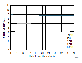
TLV6700 D008_SLVSCI7.gif
Figure 8. Supply Current (IDD) vs
Output Sink Current
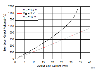
TLV6700 D010_SLVSCI7.gif
Figure 10. Output Voltage Low (VOL) vs
Output Sink Current (0°C)
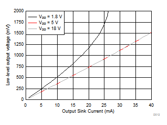
TLV6700 D012_SLVSCI7.gif
Figure 12. Output Voltage Low (VOL) vs
Output Sink Current (85°C)
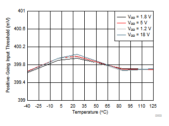
TLV6700 D003_SLVSCI7.gif
Figure 3. Rising Input Threshold Voltage (VIT+) vs Temperature
TLV6700 D005_SLVSCI7.gif
Figure 5. Propagation Delay vs Temperature
(High-to-Low Transition at the Inputs)
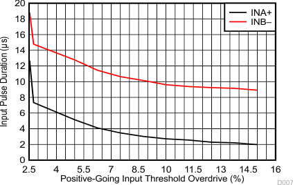
TLV6700 D007_SLVSCI7.gif
INA+ = negative spike below VIT–
INB– = positive spike above VIT+
Figure 7. Minimum Pulse Duration vs
Threshold Overdrive Voltage
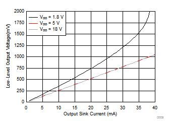
TLV6700 D009_SLVSCI7.gif
Figure 9. Output Voltage Low (VOL) vs
Output Sink Current (–40°C)
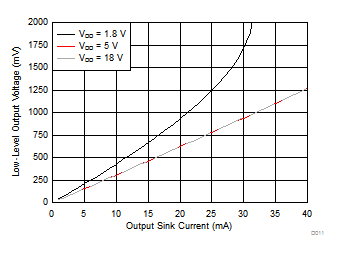
TLV6700 D011_SLVSCI7.gif
Figure 11. Output Voltage Low (VOL) vs
Output Sink Current (25°C)
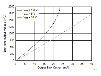
TLV6700 D013_SLVSCI7.gif
Figure 13. Output Voltage Low (VOL) vs
Output Sink Current (125°C)