ZHCSHH0B January   2018  – July 2018 TLV6713

PRODUCTION DATA.  

  1. 特性
  2. 应用
  3. 说明
    1.     Device Images
      1.      典型应用
  4. 修订历史记录
  5. Device Comparison Table
  6. Pin Configuration and Functions
    1.     Pin Functions
  7. Specifications
    1. 7.1 Absolute Maximum Ratings
    2. 7.2 ESD Ratings
    3. 7.3 Recommended Operating Conditions
    4. 7.4 Thermal Information
    5. 7.5 Electrical Characteristics
    6. 7.6 Timing Requirements
    7. 7.7 Typical Characteristics
  8. Detailed Description
    1. 8.1 Overview
    2. 8.2 Functional Block Diagram
    3. 8.3 Feature Description
      1. 8.3.1 Input Pin (SENSE)
      2. 8.3.2 Output Pin (OUT)
    4. 8.4 Device Functional Modes
      1. 8.4.1 Normal Operation (VDD > UVLO)
      2. 8.4.2 Undervoltage Lockout (V(POR) < VDD < UVLO)
      3. 8.4.3 Power On Reset (VDD < V(POR))
  9. Application and Implementation
    1. 9.1 Application Information
      1. 9.1.1 Input and Output Configurations
      2. 9.1.2 Immunity to Input Pin Voltage Transients
    2. 9.2 Typical Application
      1. 9.2.1 Design Requirements
      2. 9.2.2 Detailed Design Procedure
        1. 9.2.2.1 Resistor Divider Selection
        2. 9.2.2.2 Pullup Resistor Selection
        3. 9.2.2.3 Input Supply Capacitor
      3. 9.2.3 Application Curve
  10. 10Power Supply Recommendations
  11. 11Layout
    1. 11.1 Layout Guidelines
    2. 11.2 Layout Example
  12. 12器件和文档支持
    1. 12.1 器件支持
      1. 12.1.1 开发支持
    2. 12.2 接收文档更新通知
    3. 12.3 社区资源
    4. 12.4 商标
    5. 12.5 静电放电警告
    6. 12.6 术语表
  13. 13机械、封装和可订购信息

封装选项

机械数据 (封装 | 引脚)
散热焊盘机械数据 (封装 | 引脚)
订购信息

Typical Characteristics

at TJ = 25°C and VDD = 12 V (unless otherwise noted)
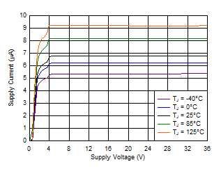
TLV6713 D001_SBVS272.gif
Figure 2. Supply Current vs Supply Voltage
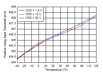
TLV6713 D002_SBVS272.gif
Figure 4. SENSE Positive Input Threshold Voltage (VIT+) vs Temperature
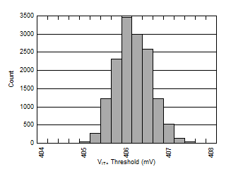
TLV6713 D012_SBVS272.gif
VDD = 1.8 V
Figure 6. SENSE Positive Input Threshold Voltage (VIT+) Distribution
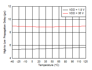
TLV6713 D005_SBVS272.gif
Input step ±200 mV
Figure 8. Propagation Delay vs Temperature
(High-to-Low Transition at SENSE)
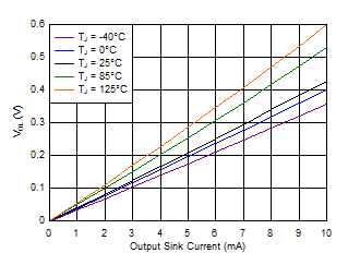
TLV6713 D009_SBVS272.gif
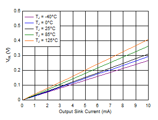
VDD = 1.8 V
Figure 10. Output Voltage Low vs Output Sink Current
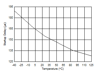
TLV6713 D008_SBVS272.gif
VDD = 5 V
Figure 12. Start-up Delay vs Temperature
TLV6713 D004_SBVS272.gif
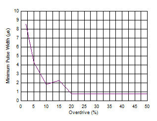
VDD = 24 V, minimum pulse duration required to trigger output high-to-low transition, SENSE = negative spike below VIT–
Figure 3. Minimum Pulse Duration vs
Threshold Overdrive Voltage
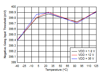
TLV6713 D003_SBVS272.gif
Figure 5. SENSE Negative Input Threshold Voltage (VIT–) vs Temperature
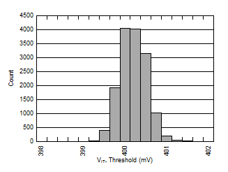
TLV6713 D011_SBVS272.gif
VDD = 1.8 V
Figure 7. SENSE Negative Input Threshold Voltage (VIT–) Distribution
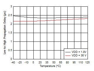
TLV6713 D006_SBVS272.gif
Input step ±200 mV
Figure 9. Propagation Delay vs Temperature
(Low-to-High Transition at SENSE)
TLV6713 D010_SBVS272.gif
VDD = 12 V
Figure 11. Output Voltage Low vs Output Sink Current