SLVSA61H February 2010 – August 2016
PRODUCTION DATA.
- 1 Features
- 2 Applications
- 3 Description
- 4 Revision History
- 5 Pin Configuration and Functions
- 6 Specifications
- 7 Detailed Description
- 8 Application and Implementation
- 9 Power Supply Recommendations
- 10Layout
- 11Device and Documentation Support
- 12Mechanical, Packaging, and Orderable Information
7 Detailed Description
7.1 Overview
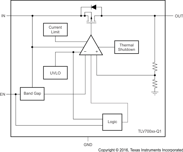
The TLV700xx-Q1 low-dropout (LDO) linear regulators are low-quiescent-current devices with excellent line- and load-transient performance. These LDOs are designed for power-sensitive applications. A precision band-gap and error amplifier provides overall 2% accuracy together with low output noise, very high power-supply rejection ratio (PSRR), and low dropout voltage.
7.3 Feature Description
7.3.1 Internal Current Limit
The TLV700xx-Q1 internal current limit helps to protect the regulator during fault conditions. During current limit, the output sources a fixed amount of current that is largely independent of the output voltage. In such a case, the output voltage is not regulated, and is VOUT = ILIMIT × RLOAD. The PMOS pass transistor dissipates (VIN – VOUT) × ILIMIT until thermal shutdown is triggered and the device turns off. As the device cools down, it is turned on by the internal thermal-shutdown circuit. If the fault condition continues, the device cycles between current limit and thermal shutdown. See the section for more details.
The PMOS pass element in the TLV700xx-Q1 has a built-in body diode that conducts current when the voltage at OUT exceeds the voltage at IN. This current is not limited, so if extended reverse voltage operation is anticipated, external limiting to 5% of the rated output current is recommended.
7.3.2 Shutdown
The enable pin (EN) is active-high and is compatible with standard and low-voltage TTL-CMOS levels. When shutdown capability is not required, EN can be connected to the IN pin.
7.3.3 Dropout Voltage
The TLV700xx-Q1 uses a PMOS pass transistor to achieve low dropout. When (VIN – VOUT) is less than the dropout voltage (VDO), the PMOS pass device is in the linear region of operation and the input-to-output resistance is the rDS(on) of the PMOS pass element. VDO scales approximately with output current because the PMOS device behaves as a resistor in dropout.
As with any linear regulator, PSRR and transient response are degraded as (VIN – VOUT) approaches dropout. This effect is shown in Figure 13 in the section.
7.3.4 Undervoltage Lockout (UVLO)
The TLV700xx-Q1 uses an undervoltage lockout circuit to keep the output shut off until internal circuitry is operating properly.
7.4 Device Functional Modes
7.4.1 Operation With VIN Less than 2 V
The TLV700xx-Q1 family of devices operates with input voltages above 2 V. The typical UVLO voltage is 1.9 V, and the device operates at an input voltage above 2 V. When input voltage falls below the UVLO voltage, the device shuts down.
7.4.2 Operation With VIN Greater than 2 V
When VIN is greater than 2 V, if the input voltage is higher than the desired output voltage plus dropout voltage, the output voltage is equal to the desired value. Otherwise, output voltage is VIN minus the dropout voltage.
