SLVSA00E September 2009 – April 2015 TLV700
PRODUCTION DATA.
- 1 Features
- 2 Applications
- 3 Description
- 4 Revision History
- 5 Pin Configuration and Functions
- 6 Specifications
- 7 Detailed Description
- 8 Application and Implementation
- 9 Power Supply Recommendations
- 10Layout
- 11Device and Documentation Support
- 12Mechanical, Packaging, and Orderable Information
封装选项
机械数据 (封装 | 引脚)
散热焊盘机械数据 (封装 | 引脚)
订购信息
8 Application and Implementation
NOTE
Information in the following applications sections is not part of the TI component specification, and TI does not warrant its accuracy or completeness. TI’s customers are responsible for determining suitability of components for their purposes. Customers should validate and test their design implementation to confirm system functionality.
8.1 Application Information
The TLV700 belongs to a new family of next-generation value LDO regulators. These devices consume low quiescent current and deliver excellent line and load transient performance. These characteristics, combined with low noise, very good PSRR with little (VIN – VOUT) headroom, make this family of devices ideal for RF portable applications. This family of regulators offers current limit and thermal protection, and is specified from –40°C to +125°C.
8.2 Typical Application
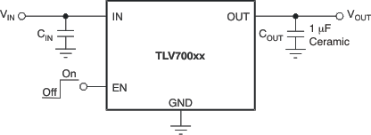
Figure 21 shows a typical application circuit.
 Figure 21. Typical Application Circuit
8.2.1 Design Requirements
Table 2 lists the design parameters.
Table 2. Design Parameters
| PARAMETER | DESIGN REQUIREMENT |
|---|---|
| Input voltage | 2.5 V to 3.3 V |
| Output voltage | 1.8 V |
| Output current | 100 mA |
8.2.2 Detailed Design Procedure
8.2.2.1 Input and Output Capacitor Requirements
TI recommends using 1-μF X5R- and X7R-type ceramic capacitors because these capacitors have minimal variation in value and equivalent series resistance (ESR) over temperature.
However, the TLV700 is designed to be stable with an effective capacitance of 0.1 μF or larger at the output. Thus, the device is stable with capacitors of other dielectric types as well, as long as the effective capacitance under operating bias voltage and temperature is greater than 0.1 μF. This effective capacitance refers to the capacitance that the LDO sees under operating bias voltage and temperature conditions; that is, the capacitance after taking both bias voltage and temperature derating into consideration. In addition to allowing the use of cheaper dielectrics, this capability of being stable with 0.1-μF effective capacitance also enables the use of smaller footprint capacitors that have higher derating in size- and space-constrained applications.
Using a 0.1-μF rated capacitor at the output of the LDO does not ensure stability because the effective capacitance under the specified operating conditions must not be less than 0.1 μF. Maximum ESR should be less than 200 mΩ.
Although an input capacitor is not required for stability, it is good analog design practice to connect a 0.1-μF to 1-μF, low ESR capacitor across the IN pin and GND in of the regulator. This capacitor counteracts reactive input sources and improves transient response, noise rejection, and ripple rejection. A higher-value capacitor may be necessary if large, fast rise-time load transients are anticipated, or if the device is not located close to the power source. If source impedance is more than 2 Ω, a 0.1-μF input capacitor may be necessary to ensure stability.
8.2.2.2 Transient Response
As with any regulator, increasing the size of the output capacitor reduces overshoot and undershoot magnitude but increases the duration of the transient response.
8.2.3 Application Curves
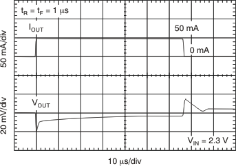
 Figure 22. TLV70018 Load Transient Response
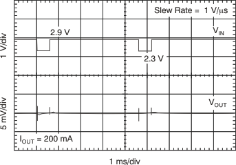
 Figure 23. TLV70018 Line Transient Response