SBVS305 March 2017 TLV703
PRODUCTION DATA.
10 Layout
10.1 Layout Guidelines
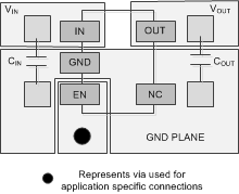
Place input and output capacitors as close to the device pins as possible. To improve ac performance (such as PSRR, output noise, and transient response), TI recommends designing the board with separate ground planes for VIN and VOUT with the ground plane connected only at the GND pin of the device. In addition, connect the ground connection for the output capacitor directly to the GND pin of the device. High ESR capacitors can degrade PSRR performance.
10.2 Layout Example
 Figure 25. Example Layout
10.3 Thermal Consideration
Thermal protection disables the output when the junction temperature rises to approximately 165°C, allowing the device to cool. When the junction temperature cools to approximately 145°C, the output circuitry is again enabled. Depending on power dissipation, thermal resistance, and ambient temperature, the thermal protection circuit can cycle on and off. This cycling limits the dissipation of the regulator, thus protecting the regulator from damage resulting from overheating.
Any tendency to activate the thermal protection circuit indicates excessive power dissipation or an inadequate heatsink. For reliable operation, limit junction temperature to 125°C maximum.
To estimate the margin of safety in a complete design (including heatsink), increase the ambient temperature until the thermal protection is triggered; use worst-case loads and signal conditions.
The internal protection circuitry of the TLV703 is designed to protect against overload conditions. This circuitry is not intended to replace proper heatsinking. Continuously running the TLV703 into thermal shutdown degrades device reliability.