ZHCSGV4H September 2017 – July 2021 TLV7031 , TLV7032 , TLV7034 , TLV7041 , TLV7042 , TLV7044
PRODUCTION DATA
- 1 特性
- 2 应用
- 3 说明
- 4 Revision History
- 5 Pin Configuration and Functions
-
6 Specifications
- 6.1 Absolute Maximum Ratings
- 6.2 ESD Ratings
- 6.3 Recommended Operating Conditions
- 6.4 Thermal Information (Single)
- 6.5 Thermal Information (Dual)
- 6.6 Thermal Information (Quad)
- 6.7 Electrical Characteristics (Single)
- 6.8 Switching Characteristics (Single)
- 6.9 Electrical Characteristics (Dual)
- 6.10 Switching Characteristics (Dual)
- 6.11 Electrical Characteristics (Quad)
- 6.12 Switching Characteristics (Quad)
- 6.13 Timing Diagrams
- 6.14 Typical Characteristics
- 7 Detailed Description
- 8 Application and Implementation
- 9 Power Supply Recommendations
- 10Layout
- 11Device and Documentation Support
- 12Mechanical, Packaging, and Orderable Information
封装选项
机械数据 (封装 | 引脚)
散热焊盘机械数据 (封装 | 引脚)
- DPW|5
订购信息
8.1.1 Inverting Comparator With Hysteresis for TLV703x
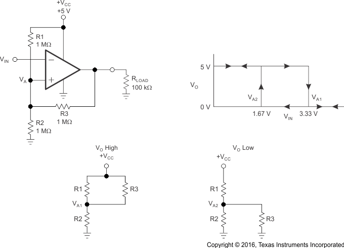
The inverting comparator with hysteresis requires a three-resistor network that is referenced to the comparator supply voltage (VCC), as shown in Figure 8-1. When VIN at the inverting input is less than VA, the output voltage is high (for simplicity, assume VO switches as high as VCC). The three network resistors can be represented as R1 || R3 in series with R2. Equation 1 defines the high-to-low trip voltage (VA1).

When VIN is greater than VA, the output voltage is low, very close to ground. In this case, the three network resistors can be presented as R2 || R3 in series with R1. Use Equation 2 to define the low to high trip voltage (VA2).

Equation 3 defines the total hysteresis provided by the network.

 Figure 8-1 TLV703x in an Inverting Configuration With Hysteresis