SBVS151F December 2010 – April 2017 TLV705 , TLV705P
PRODUCTION DATA.
8 Application and Implementation
NOTE
Information in the following applications sections is not part of the TI component specification, and TI does not warrant its accuracy or completeness. TI’s customers are responsible for determining suitability of components for their purposes. Customers should validate and test their design implementation to confirm system functionality.
8.1 Application Information
The TLV705 is a LDO that offers very low dropout voltages in a tiny package. The operating junction temperature of this device is –40°C to +125°C.
8.2 Typical Application
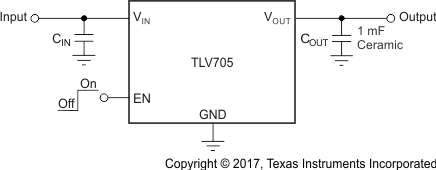
 Figure 28. Typical Application Circuit (Fixed-Voltage Versions)
8.2.1 Design Requirements
Table 2 lists the design parameters.
Table 2. Design Parameters
| PARAMETER | DESIGN REQUIREMENT |
|---|---|
| Input voltage | 2.5 V to 3.3 V |
| Output voltage | 1.8 V |
| Output current | 100 mA |
8.2.2 Detailed Design Procedure
Select the desired device based on the output voltage.
Provide an input supply with adequate headroom to account for dropout. The input supply must also provide adequate current to account for the GND pin current and load current.
8.2.2.1 Input and Output Capacitor Requirements
TI recommends using 1-μF X5R- and X7R-type ceramic capacitors because these components have minimal variation in value and equivalent series resistance (ESR) over temperature. However, the TLV705 series is designed to be stable with an effective capacitance of 0.1 μF or larger at the output. As a result, the device is stable with capacitors of other dielectrics as long as the effective capacitance under the operating bias voltage and temperature is greater than 0.1 μF. This effective capacitance refers to the capacitance that the LDO detects under operating bias voltage and temperature conditions (that is, the capacitance after taking the bias voltage and temperature derating into consideration). In addition to allowing the use of lower cost dielectrics, the effective capacitance enables using smaller footprint capacitors that have higher derating in space-constrained applications.
Using a 0.1-μF rating capacitor at the output of the LDO does not ensure stability because the effective capacitance under operating conditions is less than 0.1 μF. Maximum ESR must be less than 200 mΩ.
Although an input capacitor is not required for stability, good analog design practice is to connect a 0.1-μF to
1-μF low ESR capacitor across the VIN and GND pins of the regulator. This capacitor counteracts reactive input sources and improves transient response, noise rejection, and ripple rejection. A higher-value capacitor can be necessary if large, fast rise-time load transients are anticipated, or if the device is not located close to the power source. If source impedance is more than 2 Ω, a 0.1-μF input capacitor may be necessary to ensure stability.
8.2.2.2 Transient Response
As with any regulator, increasing the size of the output capacitor reduces overshoot and undershoot magnitude, but increases the duration of the transient response.
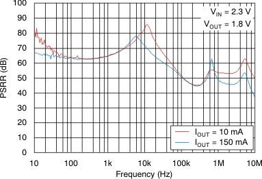
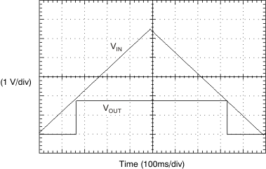
8.2.3 Application Curves


8.3 Do's and Don'ts
Place input and output capacitors as close as possible to the device.
Do not exceed the device absolute maximum ratings.