ZHCS038G february   2011  – june 2023 TLV707 , TLV707P

PRODUCTION DATA  

  1.   1
  2. 特性
  3. 应用
  4. 说明
  5. Revision History
  6. Pin Configuration and Functions
  7. Specifications
    1. 6.1 Absolute Maximum Ratings
    2. 6.2 ESD Ratings
    3. 6.3 Recommended Operating Conditions
    4. 6.4 Thermal Information
    5. 6.5 Electrical Characteristics
    6. 6.6 Typical Characteristics
  8. Detailed Description
    1. 7.1 Overview
    2. 7.2 Functional Block Diagrams
    3. 7.3 Feature Description
      1. 7.3.1 Internal Current Limit
      2. 7.3.2 Shutdown
    4. 7.4 Device Functional Modes
  9. Application and Implementation
    1. 8.1 Application Information
    2. 8.2 Typical Application
      1. 8.2.1 Design Requirements
      2. 8.2.2 Detailed Design Procedure
        1. 8.2.2.1 Input and Output Capacitor Requirements
        2. 8.2.2.2 Dropout Voltage
        3. 8.2.2.3 Transient Response
      3. 8.2.3 Application Curves
    3. 8.3 Best Design Practices
    4. 8.4 Power Supply Recommendations
    5. 8.5 Layout
      1. 8.5.1 Layout Guidelines
        1. 8.5.1.1 Board Layout Recommendations to Improve PSRR and Noise Performance
        2. 8.5.1.2 Package Mounting
        3. 8.5.1.3 Thermal Considerations
        4. 8.5.1.4 Power Dissipation
      2. 8.5.2 Layout Example
  10. Device and Documentation Support
    1. 9.1 Device Support
      1. 9.1.1 Development Support
        1. 9.1.1.1 Evaluation Modules
        2. 9.1.1.2 Spice Models
      2. 9.1.2 Device Nomenclature
    2. 9.2 Documentation Support
      1. 9.2.1 Related Documentation
    3. 9.3 接收文档更新通知
    4. 9.4 支持资源
    5. 9.5 Trademarks
    6. 9.6 静电放电警告
    7. 9.7 术语表
  11. 10Mechanical, Packaging, and Orderable Information

封装选项

机械数据 (封装 | 引脚)
散热焊盘机械数据 (封装 | 引脚)
订购信息

Pin Configuration and Functions

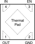
GUID-3F334233-5B52-4A1D-9417-05BF666A23F8-low.gifFigure 5-1 DQN Package,4-Pin X2SON(Top View)
Table 5-1 Pin Functions
PIN I/O DESCRIPTION
NAME NO.
EN 3 I Enable pin. Driving EN over 0.9 V turns on the regulator. Driving EN below 0.4 V puts the regulator into shutdown mode.
For TLV707P, output voltage is discharged through an internal 120-Ω resistor when device is shut down.
GND 2 Ground pin
IN 4 I Input pin. For good transient performance, place a small 1-µF ceramic capacitor from this pin to ground. See Input and Output Capacitor Requirements for more details.
OUT 1 O Regulated output voltage pin. A small 1-μF ceramic capacitor is required from this pin to ground to assure stability. See Input and Output Capacitor Requirements for more details.