ZHCSDR6 May 2015 TLV713P-Q1
PRODUCTION DATA.
6 Specifications
6.1 Absolute Maximum Ratings
Over operating junction temperature range (TJ = 25°C), unless otherwise noted. All voltages are with respect to GND.(1)| MIN | MAX | UNIT | ||
|---|---|---|---|---|
| Voltage | Input, VIN | –0.3 | 6 | V |
| Enable, VEN | –0.3 | VIN + 0.3 | V | |
| Output, VOUT | –0.3 | 3.6 | V | |
| Current | Maximum output, IOUT(max) | Internally limited | ||
| Output short-circuit duration | Indefinite | |||
| Total power dissipation | Continuous, PD(tot) | See theThermal Information | ||
| Temperature | Storage, Tstg | –55 | 150 | °C |
| Junction, TJ | –55 | 125 | °C | |
(1) Stresses beyond those listed under Absolute Maximum Ratings may cause permanent damage to the device. These are stress ratings only, which do not imply functional operation of the device at these or any other conditions beyond those indicated under Recommended Operating Conditions. Exposure to absolute-maximum-rated conditions for extended periods may affect device reliability.
6.2 ESD Ratings
| VALUE | UNIT | |||
|---|---|---|---|---|
| V(ESD) | Electrostatic discharge | Human body model (HBM), per ANSI/ESDA/JEDEC JS-001(1) | ±2000 | V |
| Charged device model (CDM), per JEDEC specification JESD22-C101(2) | ±500 | |||
(1) JEDEC document JEP155 states that 500-V HBM allows safe manufacturing with a standard ESD control process.
(2) JEDEC document JEP157 states that 250-V CDM allows safe manufacturing with a standard ESD control process.
6.3 Recommended Operating Conditions
over operating junction temperature range (unless otherwise noted).| MIN | NOM | MAX | UNIT | ||
|---|---|---|---|---|---|
| VIN | Input voltage | 1.4 | 5.5 | V | |
| VEN | Enable range | 0 | VIN | V | |
| IOUT | Output current | 0 | 150 | mA | |
| CIN | Input capacitor | 0 | 1 | µF | |
| COUT | Output capacitor | 0 | 0.1 | 100 | µF |
| TJ | Operating junction temperature range | –40 | 125 | °C | |
6.4 Thermal Information
| THERMAL METRIC | TLV713P-Q1 | UNIT | |
|---|---|---|---|
| DBV (SOT-23) | |||
| 5 PINS | |||
| RθJA | Junction-to-ambient thermal resistance | 249 | °C/W |
| RθJC(top) | Junction-to-case (top) thermal resistance | 172.7 | °C/W |
| RθJB | Junction-to-board thermal resistance | 76.7 | °C/W |
| ψJT | Junction-to-top characterization parameter | 49.7 | °C/W |
| ψJB | Junction-to-board characterization parameter | 75.8 | °C/W |
| RθJC(bot) | Junction-to-case (bottom) thermal resistance | n/a | °C/W |
6.5 Electrical Characteristics
Over operating temperature range (TJ, TA = –40°C to 125°C), VIN(nom) = VOUT(nom) + 0.5 V or VIN(nom) = 2 V (whichever is greater), IOUT = 1 mA, VEN = VIN, and COUT = 0.47 µF, unless otherwise noted. Typical values are at TJ = 25°C.| PARAMETER | TEST CONDITIONS | MIN | TYP | MAX | UNIT | ||
|---|---|---|---|---|---|---|---|
| VIN | Input voltage range | 1.4 | 5.5 | V | |||
| VOUT | Output voltage range | 1 | 3.3 | V | |||
| DC output accuracy | VOUT ≥ 1.8 V; TJ, TA = 25°C | –1% | 1% | ||||
| VOUT < 1.8 V; TJ, TA = 25°C | –20 | 20 | mV | ||||
| VOUT ≥ 1.2 V; –40°C ≤ TJ, TA ≤ 125°C | –1.5% | 1.5% | |||||
| VOUT < 1.2 V; –40°C ≤ TJ, TA ≤ 125°C | –50 | 50 | mV | ||||
| ΔVOUT(ΔVIN) | Line regulation | Max [VOUT(nom) + 0.5 V, VIN = 2.0 V] ≤ VIN ≤ 5.5 V | 1 | 5 | mV | ||
| ΔVOUT(ΔIOUT) | Load regulation | 0 mA ≤ IOUT ≤ 150 mA | 10 | 30 | mV | ||
| VDO | Dropout voltage | VOUT = 0.98 × VOUT(nom); TJ, TA = –40°C to 85°C |
1 V ≤ VOUT < 1.8 V, IOUT = 150 mA | 600 | 900 | mV | |
| 1.8 V ≤ VOUT < 2.1 V, IOUT = 30 mA | 70 | mV | |||||
| 1.8 V ≤ VOUT < 2.1 V, IOUT = 150 mA | 350 | 575 | mV | ||||
| 2.5 V ≤ VOUT < 3 V, IOUT = 30 mA | 50 | mV | |||||
| 2.5 V ≤ VOUT < 3 V, IOUT = 150 mA | 246 | 445 | mV | ||||
| 3 V ≤ VOUT < 3.6 V, IOUT = 30 mA | 46 | mV | |||||
| 3 V ≤ VOUT < 3.6 V, IOUT = 150 mA | 230 | 420 | mV | ||||
| VOUT = 0.98 × VOUT(nom); TJ, TA = –40°C to 125°C |
1 V ≤ VOUT < 1.8 V, IOUT = 150 mA | 600 | 1020 | mV | |||
| 1.8 V ≤ VOUT < 2.1 V, IOUT = 150 mA | 350 | 695 | mV | ||||
| 2.5 V ≤ VOUT < 3 V, IOUT = 150 mA | 246 | 600 | mV | ||||
| 3 V ≤ VOUT < 3.6 V, IOUT = 150 mA | 230 | 560 | mV | ||||
| IGND | Ground pin current | IOUT = 0 mA | 50 | 75 | µA | ||
| ISHUTDOWN | Shutdown current | VEN ≤ 0.4 V; 2.0 V ≤ VIN ≤ 5.5 V; TJ, TA = 25°C | 0.1 | 1 | µA | ||
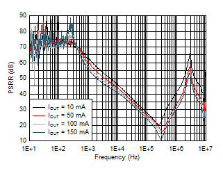
| PSRR | Power-supply rejection ratio | VIN = 3.3 V, VOUT = 2.8 V, IOUT = 30 mA |
f = 100 Hz | 70 | dB | ||
| f = 10 kHz | 55 | dB | |||||
| f = 1 MHz | 55 | dB | |||||
| Vn | Output noise voltage | BW = 100 Hz to 100 kHz, VIN = 2.3 V, VOUT = 1.8 V, IOUT = 10 mA | 73 | µVRMS | |||
| tSTR | Start-up time | COUT = 1.0 μF, IOUT = 150 mA | 100 | µs | |||
| VHI | Enable high (enabled) | 0.9 | VIN | V | |||
| VLO | Enable low (disabled) | 0 | 0.4 | V | |||
| IEN | EN pin current | EN = 5.5 V | 0.01 | µA | |||
| RPULLDOWN | Pulldown resistor | VIN = 4 V | 120 | Ω | |||
| ILIM | Output current limit | VIN = 3.8 V, VOUT = 3.3 V | 175 | mA | |||
| VIN = 3.0 V, VOUT = 2.5 V | 175 | mA | |||||
| VIN = 2.3 V, VOUT = 1.8 V | 175 | mA | |||||
| VIN = 2.0 V, VOUT = 1.2 V | 175 | mA | |||||
| VIN = 2.0 V, VOUT = 1.0 V | 175 | mA | |||||
| ISC | Short-circuit current | VOUT = 0 V | 40 | mA | |||
| TSD | Thermal shutdown | Shutdown, temperature increasing | 158 | °C | |||
| Reset, temperature decreasing | 140 | °C | |||||
6.6 Typical Characteristics
Over operating temperature range (TJ = –40°C to 125°C), VIN = VOUT(nom) + 0.5 V or 2.0 V (whichever is greater), IOUT = 10 mA, VEN = VIN, COUT = 1 µF, and VOUT(nom) = 1.8 V, unless otherwise noted. Typical values are at TJ = 25°C.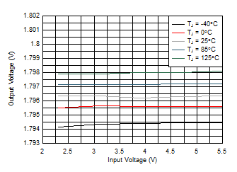
VIN and Temperature
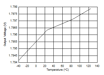
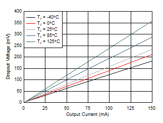
IOUT and Temperature
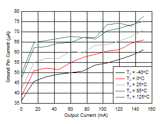
IOUT and Temperature
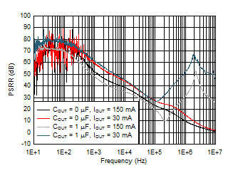
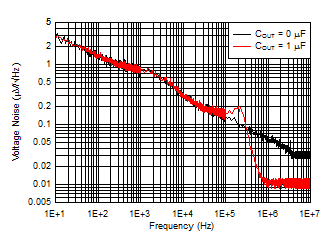
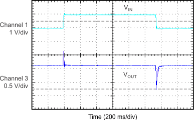
| VIN = 3 V to 4 V, IOUT = 150 mA, VOUT = 1.8 V, CIN = COUT = 0 µF |
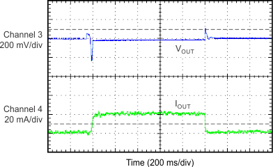
| VIN = 5 V, VOUT = 1.8 V, CIN = COUT = 0 µF |
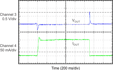
| VIN = 5 V, VOUT = 1.8 V, CIN = COUT = 0 µF |
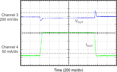
| VIN = 5 V, VOUT = 1.8 V, CIN = COUT = 0 µF |
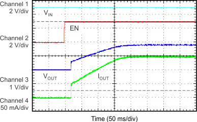
| VIN = 3 V, IOUT = 150 mA, VOUT = 1.8 V, CIN = COUT = 0 µF | ||
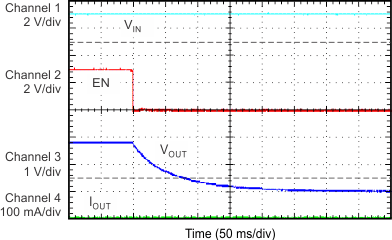
| VIN = 3 V, IOUT = 0 mA, VOUT = 1.8 V, CIN = COUT = 1 µF |
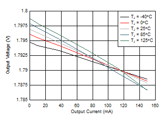
IOUT and Temperature
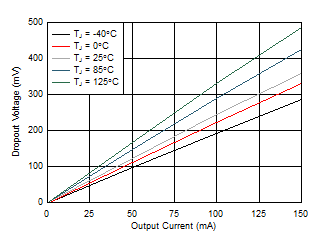
IOUT and Temperature
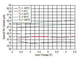
VIN and Temperature
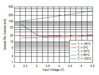
VIN and Temperature
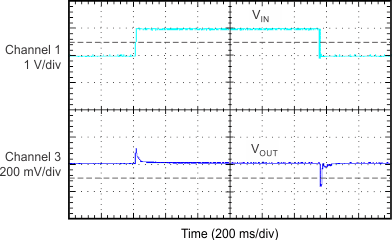
| VIN = 3 V to 4 V , IOUT = 0 mA, VOUT = 1.8 V, CIN = COUT = 0 µF |
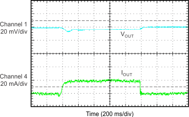
| VIN = 5 V, VOUT = 1.8 V, CIN = COUT = 1 µF |
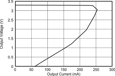
(Foldback Current Limit)
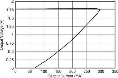
(Foldback Current Limit)
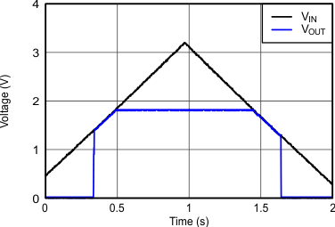
| IOUT = 150 mA |
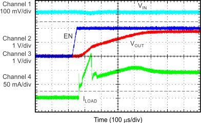
| VIN = 2.3 V, IOUT = 90 mA, COUT = 10 µF, VOUT = 1.8 V, CIN = 1 µF |