ZHCSDR6 May 2015 TLV713P-Q1
PRODUCTION DATA.
7 Detailed Description
7.1 Overview
These devices belong to a family of low-dropout (LDO) regulators that consume low quiescent current and deliver excellent line and load transient performance. These characteristics, combined with low noise and very good PSRR with little (VIN – VOUT) headroom, make this family of devices ideal for RF portable applications.
This family of regulators offers current limit and thermal protection. Device operating junction temperature is –40°C to 125°C.
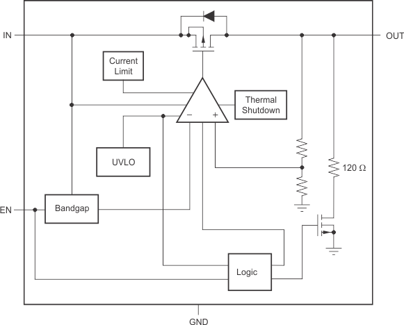
7.2 Functional Block Diagram

7.3 Feature Description
7.3.1 Undervoltage Lockout (UVLO)
The TLV713P-Q1 uses a UVLO circuit that disables the output until the input voltage is greater than the rising UVLO voltage. This circuit ensures that the device does not exhibit any unpredictable behavior when the supply voltage is lower than the operational range of the internal circuitry, VIN(min). During UVLO disable, the output of the TLV713P-Q1 is connected to ground with a 120-Ω pulldown resistor.
7.3.2 Shutdown
The enable pin (EN) is active high. Enable the device by forcing the EN pin to exceed VEN(high) (0.9 V, minimum). Turn off the device by forcing the EN pin to drop below 0.4 V. If shutdown capability is not required, connect EN to IN.
The TLV713P-Q1 has an internal pulldown MOSFET that connects a 120-Ω resistor to ground when the device is disabled. The discharge time after disabling depends on the output capacitance (COUT) and the load resistance (RL) in parallel with the 120-Ω pulldown resistor. The time constant is calculated in Equation 1.

7.3.3 Foldback Current Limit
The TLV713P-Q1 has an internal foldback current limit that helps protect the regulator during fault conditions. The current supplied by the device is gradually reduced when the output voltage decreases. When the output is shorted, the LDO supplies a typical current of 40 mA. Output voltage is not regulated when the device is in current limit, and is calculated by Equation 2:
The PMOS pass transistor dissipates [(VIN – VOUT) × ILIMIT] until thermal shutdown is triggered and the device turns off. The device is turned on by the internal thermal shutdown circuit during cool down. If the fault condition continues, the device cycles between current limit and thermal shutdown. See the Thermal Information section for more details.
The TLV713P-Q1 PMOS pass element has a built-in body diode that conducts current when the voltage at OUT exceeds the voltage at IN. This current is not limited, so if extended reverse voltage operation is anticipated, external limiting to 5% of the rated output current is recommended.
7.3.4 Thermal Protection
Thermal protection disables the output when the junction temperature rises to approximately 158°C, allowing the device to cool. When the junction temperature cools to approximately 140°C, the output circuitry is again enabled. Depending on power dissipation, thermal resistance, and ambient temperature, the thermal protection circuit may cycle on and off. This cycling limits regulator dissipation, protecting the device from damage as a result of overheating.
Any tendency to activate the thermal protection circuit indicates excessive power dissipation or an inadequate heatsink. For reliable operation, junction temperature must be limited to 125°C maximum. To estimate the margin of safety in a complete design (including heatsink), increase the ambient temperature until the thermal protection is triggered; use worst-case loads and signal conditions.
The TLV713P-Q1 internal protection circuitry is designed to protect against overload conditions. This circuitry is not intended to replace proper heatsinking. Continuously running the TLV713P-Q1 into thermal shutdown degrades device reliability.
7.4 Device Functional Modes
7.4.1 Normal Operation
The device regulates to the nominal output voltage under the following conditions:
- The input voltage is at least as high as VIN(min).
- The input voltage is greater than the nominal output voltage added to the dropout voltage.
- The enable voltage has previously exceeded the enable rising threshold voltage and has not decreased below the enable falling threshold.
- The output current is less than the current limit.
- The device junction temperature is less than the maximum specified junction temperature.
7.4.2 Dropout Operation
If the input voltage is lower than the nominal output voltage plus the specified dropout voltage, but all other conditions are met for normal operation, the device operates in dropout mode. In this mode of operation, the output voltage is the same as the input voltage minus the dropout voltage. The transient performance of the device is significantly degraded because the pass device is in the linear region and no longer controls the current through the LDO. Line or load transients in dropout can result in large output voltage deviations.
7.4.3 Disabled
The device is disabled under the following conditions:
- The enable voltage is less than the enable falling threshold voltage or has not yet exceeded the enable rising threshold.
- The device junction temperature is greater than the thermal shutdown temperature.
Table 1 shows the conditions that lead to the different modes of operation.
Table 1. Device Functional Mode Comparison
| OPERATING MODE | PARAMETER | |||
|---|---|---|---|---|
| VIN | VEN | IOUT | TJ | |
| Normal mode | VIN > VOUT(nom) + VDO and VIN > VIN(min) |
VEN > VEN(high) | IOUT < ILIM | TJ < 125°C |
| Dropout mode | VIN(min) < VIN < VOUT(nom) + VDO | VEN > VEN(high) | — | TJ < 125°C |
| Disabled mode (any true condition disables the device) |
— | VEN < VEN(low) | — | TJ > 158°C |