ZHCSD13C October   2014  – July 2019 TLV733P

PRODUCTION DATA.  

  1. 特性
  2. 应用
  3. 说明
    1.     Device Images
      1.      典型应用电路
      2.      压降电压与输出电流间的关系
  4. 修订历史记录
  5. Pin Configuration and Functions
    1.     Pin Functions
  6. Specifications
    1. 6.1 Absolute Maximum Ratings
    2. 6.2 ESD Ratings
    3. 6.3 Recommended Operating Conditions
    4. 6.4 Thermal Information
    5. 6.5 Electrical Characteristics
    6. 6.6 Typical Characteristics
  7. Detailed Description
    1. 7.1 Overview
    2. 7.2 Functional Block Diagram
    3. 7.3 Feature Description
      1. 7.3.1 Undervoltage Lockout (UVLO)
      2. 7.3.2 Shutdown and Output Enable
      3. 7.3.3 Internal Foldback Current Limit
      4. 7.3.4 Thermal Shutdown
    4. 7.4 Device Functional Modes
      1. 7.4.1 Normal Operation
      2. 7.4.2 Dropout Operation
      3. 7.4.3 Disabled
  8. Application and Implementation
    1. 8.1 Application Information
      1. 8.1.1 Input and Output Capacitor Selection
      2. 8.1.2 Dropout Voltage
      3. 8.1.3 Power Dissipation
    2. 8.2 Typical Applications
      1. 8.2.1 DC-DC Converter Post Regulation
        1. 8.2.1.1 Design Requirements
        2. 8.2.1.2 Design Considerations
        3. 8.2.1.3 Application Curve
      2. 8.2.2 Capacitor-Free Operation from Battery Input Supply
        1. 8.2.2.1 Design Requirements
        2. 8.2.2.2 Design Considerations
        3. 8.2.2.3 Application Curve
  9. Power Supply Recommendations
  10. 10Layout
    1. 10.1 Layout Guidelines
    2. 10.2 Layout Examples
  11. 11器件和文档支持
    1. 11.1 器件支持
      1. 11.1.1 开发支持
        1. 11.1.1.1 评估模块
      2. 11.1.2 器件命名规则
    2. 11.2 文档支持
      1. 11.2.1 相关文档 
    3. 11.3 接收文档更新通知
    4. 11.4 社区资源
    5. 11.5 商标
    6. 11.6 静电放电警告
    7. 11.7 Glossary
  12. 12机械、封装和可订购信息

封装选项

请参考 PDF 数据表获取器件具体的封装图。

机械数据 (封装 | 引脚)
  • DBV|5
  • DQN|4
散热焊盘机械数据 (封装 | 引脚)
订购信息

Pin Configuration and Functions

DBV Package
5-Pin SOT-23
Top View
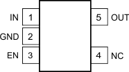
TLV733P po_sot23_bvs195.gif
DQN Package
4-Pin 1-mm × 1-mm X2SON
Top View
TLV733P po_dfn_dpw_bvs195.gif

Pin Functions

PIN I/O DESCRIPTION
NAME NO.
DQN DBV
EN 3 3 I Enable pin. Drive EN greater than VEN(HI) to turn on the regulator.
Drive EN less than VEN(LO) to put the LDO into shutdown mode.
GND 2 2 Ground pin
IN 4 1 I Input pin. A small capacitor is recommended from this pin to ground.
See the Input and Output Capacitor Selection section for more details.
NC N/A 4 No internal connection
OUT 1 5 O Regulated output voltage pin. For best transient response, use a small 1-μF ceramic capacitor from this pin to ground.
See the Input and Output Capacitor Selectionsection for more details.
Thermal pad The thermal pad is electrically connected to the GND node.
Connect to the GND plane for improved thermal performance.