ZHCSGP8 September   2017 TLV742P

PRODUCTION DATA.  

  1. 特性
  2. 应用
  3. 说明
  4. 修订历史记录
  5. Pin Configuration and Functions
  6. Specifications
    1. 6.1 Absolute Maximum Ratings
    2. 6.2 ESD Ratings
    3. 6.3 Recommended Operating Conditions
    4. 6.4 Thermal Information
    5. 6.5 Electrical Characteristics
    6. 6.6 Typical Characteristics
  7. Detailed Description
    1. 7.1 Overview
    2. 7.2 Functional Block Diagrams
    3. 7.3 Feature Description
      1. 7.3.1 Internal Current Limit
      2. 7.3.2 Shutdown
    4. 7.4 Device Functional Modes
  8. Application and Implementation
    1. 8.1 Application Information
    2. 8.2 Typical Application
      1. 8.2.1 Design Requirements
      2. 8.2.2 Detailed Design Procedure
        1. 8.2.2.1 Input and Output Capacitor Requirements
        2. 8.2.2.2 Dropout Voltage
        3. 8.2.2.3 Transient Response
      3. 8.2.3 Application Curves
    3. 8.3 Do's and Don'ts
  9. Power Supply Recommendations
  10. 10Layout
    1. 10.1 Layout Guidelines
      1. 10.1.1 Board Layout Recommendations to Improve PSRR and Noise Performance
      2. 10.1.2 Package Mounting
    2. 10.2 Layout Example
    3. 10.3 Thermal Considerations
    4. 10.4 Power Dissipation
  11. 11器件和文档支持
    1. 11.1 器件支持
      1. 11.1.1 开发支持
        1. 11.1.1.1 评估模块
      2. 11.1.2 器件命名规则
    2. 11.2 接收文档更新通知
    3. 11.3 社区资源
    4. 11.4 商标
    5. 11.5 静电放电警告
    6. 11.6 Glossary
  12. 12机械、封装和可订购信息

封装选项

机械数据 (封装 | 引脚)
散热焊盘机械数据 (封装 | 引脚)
订购信息

Pin Configuration and Functions

DQN Package
4-Pin X2SON With Exposed Thermal Pad
Top View
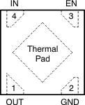
TLV742P po_dqn_bvs153.gif

Pin Functions

PIN I/O DESCRIPTION
NAME NO.
EN 3 I Enable pin. Driving EN over 0.9 V turns on the regulator. Driving EN below 0.4 V puts the regulator into shutdown mode.
For TLV742P, output voltage is discharged through an internal 120-Ω resistor when device is shut down.
GND 2 Ground pin
IN 4 I Input pin. For good transient performance, place a small 1-µF ceramic capacitor from this pin to ground. See Input and Output Capacitor Requirements for more details.
OUT 1 O Regulated output voltage pin. A small 1-μF ceramic capacitor is required from this pin to ground to ensure stability. See Input and Output Capacitor Requirements for more details.
Thermal pad The thermal pad is electrically connected to the GND node. Connect to the GND plane for improved thermal performance.