ZHCSGP8 September 2017 TLV742P
PRODUCTION DATA.
7 Detailed Description
7.1 Overview
The TLV742P device belongs to a family of LDOs. This device consumes low quiescent current and delivers excellent line and load transient performance. These characteristics [combined with low noise and very good PSRR with little (VIN – VOUT) headroom] make this device ideal for portable RF applications.
7.2 Functional Block Diagrams
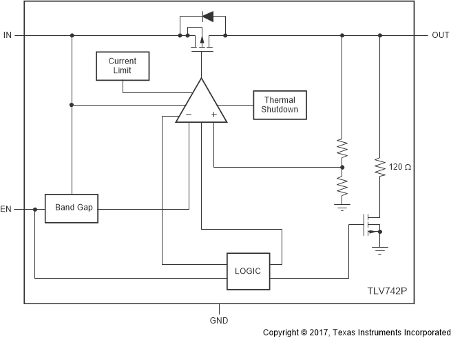
 Figure 43. TLV742P Block Diagram
7.3 Feature Description
This LDO regulator offers current limit and thermal protection. The operating junction temperature of this device is –40°C to +125°C.
7.3.1 Internal Current Limit
The internal current limit helps to protect the regulator during fault conditions. During current limit, the output sources a fixed amount of current that is largely independent of the output voltage. In such a case, the output voltage is not regulated, and is VOUT = ICL × RL. The PMOS pass transistor dissipates (VIN – VOUT) × ILIMIT until thermal shutdown is triggered and the device turns off. When the device cools, the internal thermal shutdown circuit turns the device back on. If the fault condition continues, the device cycles between current limit and thermal shutdown; see Thermal Information for more details.
The PMOS pass element has a built-in body diode that conducts current when the voltage at OUT exceeds the voltage at IN. This current is not limited, so if extended reverse voltage operation is anticipated, external limiting to 5% of the rated output current is recommended.
7.3.2 Shutdown
The enable pin (EN) is active high. The device is enabled when voltage at the EN pin goes above 0.9 V. The device is turned off when the EN pin is held at less than 0.4 V. When shutdown capability is not required, EN can be connected to the IN pin.
The TLV742P version has internal active pulldown circuitry that discharges the output with a time constant as given by Equation 1:

where
- RL = Load resistance
- COUT = Output capacitor
7.4 Device Functional Modes
The TLV742P series is specified over the recommended operating conditions (see Recommended Operating Conditions). The specifications may not be met when exposed to conditions outside of the recommended operating range.
To turn on the regulator, the EN pin must be driven over 0.9 V. Driving the EN pin below 0.4 V causes the regulator to enter shutdown mode.
In shutdown, the current consumption of the device typically reduces to 1 µA.