ZHCSHZ7A April   2018  – December 2018 TLV759P

PRODUCTION DATA.  

  1. 特性
  2. 应用
  3. 说明
    1.     Device Images
      1.      典型应用
  4. 修订历史记录
  5. Pin Configuration and Functions
    1.     Pin Functions
  6. Specifications
    1. 6.1 Absolute Maximum Ratings
    2. 6.2 ESD Ratings
    3. 6.3 Recommended Operating Conditions
    4. 6.4 Thermal Information
    5. 6.5 Electrical Characteristics
    6. 6.6 Typical Characteristics
  7. Detailed Description
    1. 7.1 Overview
    2. 7.2 Functional Block Diagram
    3. 7.3 Feature Description
      1. 7.3.1 Undervoltage Lockout (UVLO)
      2. 7.3.2 Shutdown
      3. 7.3.3 Foldback Current Limit
      4. 7.3.4 Thermal Shutdown
    4. 7.4 Device Functional Modes
      1. 7.4.1 Device Functional Mode Comparison
      2. 7.4.2 Normal Operation
      3. 7.4.3 Dropout Operation
      4. 7.4.4 Disabled
  8. Application and Implementation
    1. 8.1 Application Information
      1. 8.1.1 Adjustable Device Feedback Resistors
      2. 8.1.2 Input and Output Capacitor Selection
      3. 8.1.3 Dropout Voltage
      4. 8.1.4 Exiting Dropout
      5. 8.1.5 Reverse Current
      6. 8.1.6 Power Dissipation (PD)
    2. 8.2 Feed-Forward Capacitor (CFF)
    3. 8.3 Typical Application
      1. 8.3.1 Design Requirements
      2. 8.3.2 Detailed Design Procedure
        1. 8.3.2.1 Input Current
        2. 8.3.2.2 Thermal Dissipation
      3. 8.3.3 Application Curve
  9. Power Supply Recommendations
  10. 10Layout
    1. 10.1 Layout Guidelines
    2. 10.2 Layout Example
  11. 11器件和文档支持
    1. 11.1 文档支持
      1. 11.1.1 相关文档
    2. 11.2 接收文档更新通知
    3. 11.3 社区资源
    4. 11.4 商标
    5. 11.5 静电放电警告
    6. 11.6 术语表
  12. 12机械、封装和可订购信息

封装选项

机械数据 (封装 | 引脚)
散热焊盘机械数据 (封装 | 引脚)
订购信息

Reverse Current

As with most LDOs, excessive reverse current can damage this device.

Reverse current flows through the body diode on the pass element instead of the normal conducting channel. At high magnitudes, this current flow degrades the long-term reliability of the device, as a result of one of the following conditions:

  • Degradation caused by electromigration
  • Excessive heat dissipation
  • Potential for a latch-up condition

Conditions where reverse current can occur are outlined in this section, all of which can exceed the absolute maximum rating of VOUT > VIN + 0.3 V:

  • If the device has a large COUT and the input supply collapses with little or no load current
  • The output is biased when the input supply is not established
  • The output is biased above the input supply

If reverse current flow is expected in the application, external protection must be used to protect the device. Figure 43 shows one approach of protecting the device.
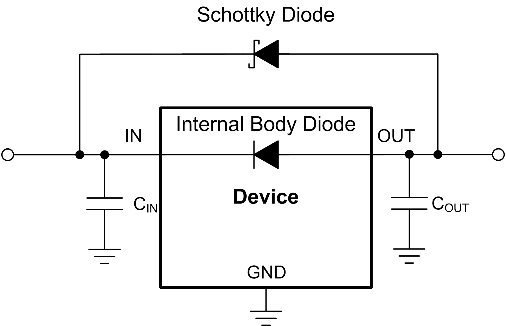
TLV759P ai_reverse_current_soln_sbvs267.gifFigure 43. Example Circuit for Reverse Current Protection Using a Schottky Diode