ZHCSJ62D December   2017  – July 2021 TLV767

PRODUCTION DATA  

  1. 特性
  2. 应用
  3. 说明
  4. Revision History
  5. Pin Configuration and Functions
  6. Specifications
    1. 6.1 Absolute Maximum Ratings
    2. 6.2 ESD Ratings
    3. 6.3 Recommended Operating Conditions
    4. 6.4 Thermal Information
    5. 6.5 Electrical Characteristics
  7. Typical Characteristics
  8. Detailed Description
    1. 8.1 Overview
    2. 8.2 Functional Block Diagrams
    3. 8.3 Feature Description
      1. 8.3.1 Output Enable
      2. 8.3.2 Dropout Voltage
      3. 8.3.3 Foldback Current Limit
      4. 8.3.4 Undervoltage Lockout (UVLO)
      5. 8.3.5 Output Pulldown
      6. 8.3.6 Thermal Shutdown
    4. 8.4 Device Functional Modes
      1. 8.4.1 Device Functional Mode Comparison
      2. 8.4.2 Normal Operation
      3. 8.4.3 Dropout Operation
      4. 8.4.4 Disabled
  9. Application and Implementation
    1. 9.1 Application Information
      1. 9.1.1 Adjustable Device Feedback Resistors
      2. 9.1.2 Recommended Capacitor Types
      3. 9.1.3 Input and Output Capacitor Requirements
      4. 9.1.4 Reverse Current
      5. 9.1.5 Feed-Forward Capacitor (CFF)
      6. 9.1.6 Power Dissipation (PD)
      7. 9.1.7 Estimating Junction Temperature
    2. 9.2 Typical Application
      1. 9.2.1 Design Requirements
      2. 9.2.2 Detailed Design Procedure
        1. 9.2.2.1 Transient Response
        2. 9.2.2.2 Choose Feedback Resistors
      3. 9.2.3 Application Curves
  10. 10Power Supply Recommendations
  11. 11Layout
    1. 11.1 Layout Guidelines
    2. 11.2 Layout Examples
  12. 12Device and Documentation Support
    1. 12.1 Device Support
      1. 12.1.1 Device Nomenclature
    2. 12.2 Documentation Support
      1. 12.2.1 Related Documentation
    3. 12.3 接收文档更新通知
    4. 12.4 支持资源
    5. 12.5 Trademarks
    6. 12.6 Electrostatic Discharge Caution
    7. 12.7 术语表

封装选项

机械数据 (封装 | 引脚)
散热焊盘机械数据 (封装 | 引脚)
订购信息

Application Curves

GUID-4E0C95F3-D90A-4662-8034-EC165CDCAE23-low.gif
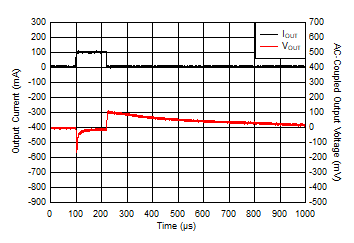
VIN = 5 V, VOUT = 3.3 V, COUT = 1 µF, CFF = 10 pF
Figure 9-3 Load Transient Response, IOUT 0 mA to 100 mA
GUID-C2CB856F-7913-48BD-9862-563849AC9FA6-low.gif
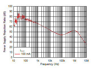
VIN = 5 V, VOUT = 3.3 V, COUT = 1 µF, CFF = 0 pF
Figure 9-4 PSRR Performance