ZHCSJX8J August   2018  – May 2021 TLV803E , TLV809E , TLV810E

PRODMIX  

  1. 特性
  2. 应用
  3. 说明
  4. Revision History
  5. Device Comparison
  6. Pin Configuration and Functions
  7. Specifications
    1. 7.1 Absolute Maximum Ratings
    2. 7.2 ESD Ratings
    3. 7.3 Recommended Operating Conditions
    4. 7.4 Thermal Information
    5. 7.5 Electrical Characteristics
    6. 7.6 Timing Requirements
    7. 7.7 Timing Diagrams
    8. 7.8 Typical Characteristics
  8. Detailed Description
    1. 8.1 Overview
    2. 8.2 Functional Block Diagram
    3. 8.3 Feature Description
      1. 8.3.1 Input Voltage (VDD)
      2. 8.3.2 VDD Hysteresis
      3. 8.3.3 VDD Glitch Immunity
      4. 8.3.4 Manual Reset (MR) Input for X2SON (DPW) Package Only
      5. 8.3.5 Output Logic
        1. 8.3.5.1 RESET Output, Active-Low
        2. 8.3.5.2 RESET Output, Active-High
    4. 8.4 Device Functional Modes
      1. 8.4.1 Normal Operation (VDD > VDD(min))
      2. 8.4.2 VDD Between VPOR and VDD(min)
      3. 8.4.3 Below Power-On-Reset (VDD < VPOR)
  9. Application and Implementation
    1. 9.1 Application Information
    2. 9.2 Typical Application - Voltage Rail Monitoring
      1. 9.2.1 Design Requirements
      2. 9.2.2 Detailed Design Procedure
      3. 9.2.3 Application Curves
    3. 9.3 Typical Application - Overvoltage Monitoring
      1. 9.3.1 Design Requirements
      2. 9.3.2 Detailed Design Procedure
  10. 10Power Supply Recommendations
  11. 11Layout
    1. 11.1 Layout Guidelines
    2. 11.2 Layout Example
  12. 12Device and Documentation Support
    1. 12.1 Device Support
      1. 12.1.1 Device Nomenclature
    2. 12.2 Documentation Support
      1. 12.2.1 Related Documentation
    3. 12.3 接收文档更新通知
    4. 12.4 支持资源
    5. 12.5 Trademarks
    6. 12.6 Electrostatic Discharge Caution
    7. 12.7 术语表
  13. 13Mechanical, Packaging, and Orderable Information

封装选项

机械数据 (封装 | 引脚)
散热焊盘机械数据 (封装 | 引脚)
订购信息

Application Curves

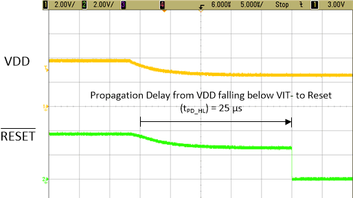
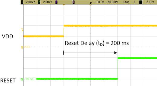
Figure 9-2 and Figure 9-3 show the TLV803EA29 functionality. In Figure 9-2, the VDD supply voltage drops from 30% above VIT- = 3.8 V to 10% below VIT- = 2.6 V with a 0.1-µF capacitor on VDD. The RESET output is connected to VDD through the pull-up resistor so when the VDD supply voltage drops. The RESET output discharges down to the VDD supply voltage through the pull-up resistor and RESET pin capacitance. Once the high-to-low propagation delay tPD_HL expires, the internal MOSFET turns on and asserts RESET to logic low. Note that tPD_HL varies with VDD specifically on how much VDD drops and how quickly in addition to the VDD and RESET pin capacitances. In Figure 9-3, VDD rises from 2 V to 4 V and the RESET output deasserts to logic high after the reset delay time (tD) expires.
GUID-D8129DB5-CDA4-4E18-8876-7B0A26037702-low.gif
Figure 9-2 Propagation Delay when Fault Occurs after VDD Falls Below VIT- (TLV803EA29 No Load) (1) (2)
GUID-7E92D25A-97E6-44FA-9606-643B1F078C6A-low.gif
Figure 9-3 RESET Delay when Returning from Fault after VDD Rises Above VIT+ (TLV803EA29)
  1. Typical tPD_HL= 30 µs for VDD falling from (VIT+ + 30%) to (VIT- - 10%).
  2. VDD does not fall all the way to 0 V so RESET momentarily discharges to VDD until tPD_HL expires.