ZHCSI62J August 2018 – February 2024 TLV9051 , TLV9052 , TLV9054
PRODUCTION DATA
- 1
- 1 特性
- 2 应用
- 3 说明
- 4 Device Comparison Table
- 5 Pin Configuration and Functions
-
6 Specifications
- 6.1 Absolute Maximum Ratings
- 6.2 ESD Ratings
- 6.3 Recommended Operating Conditions
- 6.4 Thermal Information for Single Channel
- 6.5 Thermal Information for Dual Channel
- 6.6 Thermal Information for Quad Channel
- 6.7 Electrical Characteristics: VS (Total Supply Voltage) = (V+) – (V–) = 1.8 V to 5.5 V
- 6.8 Typical Characteristics
- 7 Detailed Description
- 8 Application and Implementation
- 9 Device and Documentation Support
- 10Revision History
- 11Mechanical, Packaging, and Orderable Information
封装选项
机械数据 (封装 | 引脚)
散热焊盘机械数据 (封装 | 引脚)
- DPW|5
订购信息
7.3.7 Electrical Overstress
Designers often ask questions about the capability of an operational amplifier to withstand electrical overstress. These questions tend to focus on the device inputs, but can involve the supply voltage pins or even the output pin. Each of these different pin functions have electrical stress limits determined by the voltage breakdown characteristics of the particular semiconductor fabrication process and specific circuits connected to the pin. Additionally, internal electrostatic discharge (ESD) protection is built into these circuits to protect them from accidental ESD events both before and during product assembly.
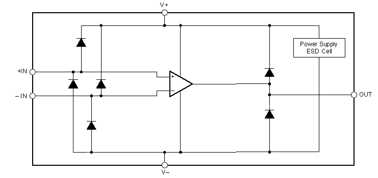
Having a good understanding of this basic ESD circuitry and its relevance to an electrical overstress event is helpful. Figure 7-2 shows the ESD circuits contained in the TLV905x devices. The ESD protection circuitry involves several current-steering diodes connected from the input and output pins and routed back to the internal power supply lines, where they meet at an absorption device internal to the operational amplifier. This protection circuitry is intended to remain inactive during normal circuit operation.
 Figure 7-2 Equivalent Internal ESD Circuitry