ZHCSUZ6B February   2024  – May 2024 TLV9051-Q1 , TLV9052-Q1

PRODMIX  

  1.   1
  2. 特性
  3. 应用
  4. 说明
  5. Pin Configuration and Functions
  6. Specifications
    1. 5.1 Absolute Maximum Ratings
    2. 5.2 ESD Ratings
    3. 5.3 Recommended Operating Conditions
    4. 5.4 Thermal Information for Single Channel
    5. 5.5 Thermal Information for Dual Channel
    6. 5.6 Thermal Information for Quad Channel
    7. 5.7 Electrical Characteristics: VS (Total Supply Voltage) = (V+) – (V–) = 1.8V to 5.5V
    8. 5.8 Typical Characteristics
  7. Detailed Description
    1. 6.1 Overview
    2. 6.2 Functional Block Diagram
    3. 6.3 Feature Description
      1. 6.3.1 Operating Voltage
      2. 6.3.2 Rail-to-Rail Input
      3. 6.3.3 Rail-to-Rail Output
      4. 6.3.4 EMI Rejection
      5. 6.3.5 Overload Recovery
      6. 6.3.6 Electrical Overstress
      7. 6.3.7 Input Protection
    4. 6.4 Device Functional Modes
  8. Application and Implementation
    1. 7.1 Application Information
    2. 7.2 Typical Low-Side Current Sense Application
      1. 7.2.1 Design Requirements
      2. 7.2.2 Detailed Design Procedure
      3. 7.2.3 Application Curve
    3. 7.3 Power Supply Recommendations
    4. 7.4 Layout
      1. 7.4.1 Layout Guidelines
      2. 7.4.2 Layout Example
  9. Device and Documentation Support
    1. 8.1 器件支持
      1. 8.1.1 开发支持
        1. 8.1.1.1 TINA-TI(免费软件下载)
    2. 8.2 Documentation Support
      1. 8.2.1 Related Documentation
    3. 8.3 接收文档更新通知
    4. 8.4 支持资源
    5. 8.5 商标
    6. 8.6 静电放电警告
    7. 8.7 术语表
  10. Revision History
  11. 10Mechanical, Packaging, and Orderable Information

封装选项

请参考 PDF 数据表获取器件具体的封装图。

机械数据 (封装 | 引脚)
  • PW|8
散热焊盘机械数据 (封装 | 引脚)
订购信息

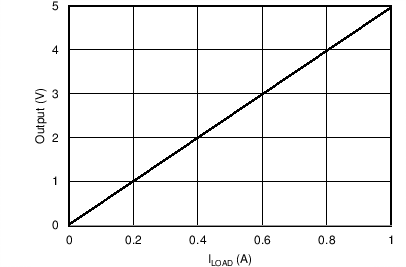
Application Curve

TLV9051-Q1 TLV9052-Q1 Low-Side, Current-Sense Transfer Function
Figure 7-2 Low-Side, Current-Sense Transfer Function