ZHCSL96A June 2020 – October 2020 TMAG5124
PRODUCTION DATA
- 1
- 1 特性
- 2 应用
- 3 说明
- 4 Revision History
- 5 Device Comparison Table
- 6 Pin Configuration and Functions
-
7 Specifications
- 7.1 Absolute Maximum Ratings
- 7.2 ESD Ratings
- 7.3 Recommended Operating Conditions
- 7.4 Thermal Information
- 7.5 Electrical Characteristics
- 7.6 Magnetic Characteristics
- 7.7 Typical Characteristics
- 8 Detailed Description
- 9 Application and Implementation
- 10Power Supply Recommendations
- 11Layout
- 12Device and Documentation Support
- 13Mechanical, Packaging, and Orderable Information
10.1 Power Derating
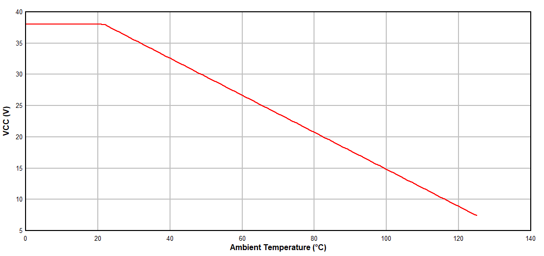
The device is specified from –40 °C to 125 °C for a voltage rating of 2.5 V to 38 V. The part drains at its maximum current of 17 mA, therefore the maximum voltage that can be applied to the device will depend on what maximum ambient temperature is acceptable for the application. The curve in Figure 10-1 shows the maximum acceptable power supply voltage versus the maximum acceptable ambient temperature.
Use Equation 3, Equation 4, and Equation 5 to populate the data shown in Figure 10-1:

where
- TJ is the junction temperature.
- TA is the ambient temperature.
- ΔT is the difference between the junction temperature and the ambient temperature.

where
- PD is the power dissipated by the part.
- RθJA is the junction to ambient thermal resistance.

where
- VCC is the voltage supply of the device.
- ICC is the current consumption of the device.
Combining these equations gives Equation 6, which can be used to determine the maximum voltage the part can handle in regards of the ambient temperature.

For example, if an application must work under an ambient temperature maximum of 100 °C, and the TJ max, RθJA and ICC max are the same values defined in the data sheet, then the maximum voltage allowed for this application is calculated in Equation 7:

 Figure 10-1 Power Derating Curve