ZHCSM20 June   2021 TMCS1100-Q1

PRODUCTION DATA  

  1. 特性
  2. 应用
  3. 说明
  4. Revision History
  5. Device Comparison
  6. Pin Configuration and Functions
  7. Specifications
    1. 7.1  Absolute Maximum Ratings
    2. 7.2  ESD Ratings
    3. 7.3  Recommended Operating Conditions
    4. 7.4  Thermal Information
    5. 7.5  Power Ratings
    6. 7.6  Insulation Specifications
    7. 7.7  Safety-Related Certifications
    8. 7.8  Safety Limiting Values
    9. 7.9  Electrical Characteristics
    10. 7.10 Typical Characteristics
      1. 7.10.1 Insulation Characteristics Curves
  8. Parameter Measurement Information
    1. 8.1 Accuracy Parameters
      1. 8.1.1 Sensitivity Error
      2. 8.1.2 Offset Error and Offset Error Drift
      3. 8.1.3 Nonlinearity Error
      4. 8.1.4 Power Supply Rejection Ratio
      5. 8.1.5 Common-Mode Rejection Ratio
      6. 8.1.6 Reference Voltage Rejection Ratio
      7. 8.1.7 External Magnetic Field Errors
    2. 8.2 Transient Response Parameters
      1. 8.2.1 Slew Rate
      2. 8.2.2 Propagation Delay and Response Time
      3. 8.2.3 Current Overload Parameters
      4. 8.2.4 CMTI, Common-Mode Transient Immunity
    3. 8.3 Safe Operating Area
      1. 8.3.1 Continuous DC or Sinusoidal AC Current
      2. 8.3.2 Repetitive Pulsed Current SOA
      3. 8.3.3 Single Event Current Capability
  9. Detailed Description
    1. 9.1 Overview
    2. 9.2 Functional Block Diagram
    3. 9.3 Feature Description
      1. 9.3.1 Current Input
      2. 9.3.2 Input Isolation
      3. 9.3.3 High-Precision Signal Chain
        1. 9.3.3.1 Temperature Stability
        2. 9.3.3.2 Lifetime and Environmental Stability
        3. 9.3.3.3 Frequency Response
        4. 9.3.3.4 Transient Response
      4. 9.3.4 External Reference Voltage Input
      5. 9.3.5 Current-Sensing Measurable Ranges
    4. 9.4 Device Functional Modes
      1. 9.4.1 Power-Down Behavior
  10. 10Application and Implementation
    1. 10.1 Application Information
      1. 10.1.1 Total Error Calculation Examples
        1. 10.1.1.1 Room Temperature Error Calculations
        2. 10.1.1.2 Full Temperature Range Error Calculations
    2. 10.2 Typical Application
      1. 10.2.1 Design Requirements
      2. 10.2.2 Detailed Design Procedure
  11. 11Power Supply Recommendations
  12. 12Layout
    1. 12.1 Layout Guidelines
    2. 12.2 Layout Example
  13. 13Device and Documentation Support
    1. 13.1 Device Support
      1. 13.1.1 Development Support
    2. 13.2 Documentation Support
      1. 13.2.1 Related Documentation
    3. 13.3 接收文档更新通知
    4. 13.4 支持资源
    5. 13.5 Trademarks
    6. 13.6 Electrostatic Discharge Caution
    7. 13.7 术语表
  14. 14Mechanical, Packaging, and Orderable Information

封装选项

机械数据 (封装 | 引脚)
散热焊盘机械数据 (封装 | 引脚)
订购信息

Transient Response Parameters

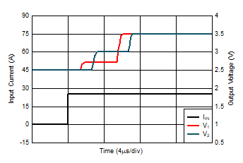
The transient response of the TMCS1100-Q1 is impacted by the 250 kHz sampling rate as defined in Section 9.3.3.4. Figure 8-2 shows the TMCS1100-Q1 response to an input current step sufficient to generate a 1V output change. The typical 4us sampling window can be observed as a periodic step. This sampling window dominates the response of the device, and the response will have some probabilistic nature due to alignment of the input step and the sampling window interval.
GUID-9670F89B-363F-4D98-9626-7256E355DBBE-low.gifFigure 8-2 Transient Step Response