ZHCSK83B September   2019  – July 2021 TMCS1100

PRODUCTION DATA  

  1. 特性
  2. 应用
  3. 说明
  4. Revision History
  5. Device Comparison
  6. Pin Configuration and Functions
  7. Specifications
    1. 7.1  Absolute Maximum Ratings
    2. 7.2  ESD Ratings
    3. 7.3  Recommended Operating Conditions
    4. 7.4  Thermal Information
    5. 7.5  Power Ratings
    6. 7.6  Insulation Specifications
    7. 7.7  Safety-Related Certifications
    8. 7.8  Safety Limiting Values
    9. 7.9  Electrical Characteristics
    10. 7.10 Typical Characteristics
      1. 7.10.1 Insulation Characteristics Curves
  8. Parameter Measurement Information
    1. 8.1 Accuracy Parameters
      1. 8.1.1 Sensitivity Error
      2. 8.1.2 Offset Error and Offset Error Drift
      3. 8.1.3 Nonlinearity Error
      4. 8.1.4 Power Supply Rejection Ratio
      5. 8.1.5 Common-Mode Rejection Ratio
      6. 8.1.6 Reference Voltage Rejection Ratio
      7. 8.1.7 External Magnetic Field Errors
    2. 8.2 Transient Response Parameters
      1. 8.2.1 Slew Rate
      2. 8.2.2 Propagation Delay and Response Time
      3. 8.2.3 Current Overload Parameters
      4. 8.2.4 CMTI, Common-Mode Transient Immunity
    3. 8.3 Safe Operating Area
      1. 8.3.1 Continuous DC or Sinusoidal AC Current
      2. 8.3.2 Repetitive Pulsed Current SOA
      3. 8.3.3 Single Event Current Capability
  9. Detailed Description
    1. 9.1 Overview
    2. 9.2 Functional Block Diagram
    3. 9.3 Feature Description
      1. 9.3.1 Current Input
      2. 9.3.2 Input Isolation
      3. 9.3.3 High-Precision Signal Chain
        1. 9.3.3.1 Temperature Stability
        2. 9.3.3.2 Lifetime and Environmental Stability
        3. 9.3.3.3 Frequency Response
        4. 9.3.3.4 Transient Response
      4. 9.3.4 External Reference Voltage Input
      5. 9.3.5 Current-Sensing Measurable Ranges
    4. 9.4 Device Functional Modes
      1. 9.4.1 Power-Down Behavior
  10. 10Application and Implementation
    1. 10.1 Application Information
      1. 10.1.1 Total Error Calculation Examples
        1. 10.1.1.1 Room Temperature Error Calculations
        2. 10.1.1.2 Full Temperature Range Error Calculations
    2. 10.2 Typical Application
      1. 10.2.1 Design Requirements
      2. 10.2.2 Detailed Design Procedure
      3. 10.2.3 Application Curve
  11. 11Power Supply Recommendations
  12. 12Layout
    1. 12.1 Layout Guidelines
    2. 12.2 Layout Example
  13. 13Device and Documentation Support
    1. 13.1 Device Support
      1. 13.1.1 Development Support
    2. 13.2 Documentation Support
      1. 13.2.1 Related Documentation
    3. 13.3 接收文档更新通知
    4. 13.4 支持资源
    5. 13.5 Trademarks
    6. 13.6 Electrostatic Discharge Caution
    7. 13.7 术语表
  14. 14Mechanical, Packaging, and Orderable Information

封装选项

机械数据 (封装 | 引脚)
散热焊盘机械数据 (封装 | 引脚)
订购信息

Full Temperature Range Error Calculations

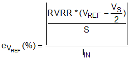
To calculate total error across any specific temperature range, Equation 26 and Equation 27 should be used for RSS maximum total errors, similar to the example for room temperatures. Conditions from the example in Section 10.1.1.1 have been replaced with their respective equations and error components for a
–40°C to 85°C temperature range below in Table 10-2.

Table 10-2 Total Error Calculation: –40°C to 85°C Example
ERROR COMPONENTSYMBOLEQUATION% MAX TOTAL ERROR AT IIN = 25 A% MAX TOTAL ERROR AT IIN = 12.5 A
Input offset erroreIos,ΔT
GUID-4325DA35-B9AF-4792-80D1-380480322DFE-low.gif
0.28%0.56%
PSRR errorePSRR
GUID-3AA116C0-74C8-4D8A-B168-0C9CE810BD64-low.gif
0.27%0.54%
CMRR error eCMRR
GUID-39A8E4F2-2B53-4187-999D-E55E58FE45E8-low.gif
0.01% 0.02%
VREF erroreVREF
GUID-587E8D46-739F-4EA2-A9B9-CC009BC5DB3B-low.gif
0.04%0.08%
External Field erroreBext
GUID-6E76128A-ED11-4990-9CC9-F72147E3F9D7-low.gif
0.11%0.22%
Sensitivity erroreS,ΔTSpecified in Section 7.90.85%0.85%
Nonlinearity erroreNLSpecified in Section 7.90.05%0.05%
RSS total erroreRSS,ΔT
GUID-1B1D1EA8-A3EE-44ED-A530-D35A94F9A548-low.gif
1.03%1.43%